This entry tries to answer questions on how the input beam RIN is coupling to the sensitivity, and how it is included in the simulink noise budget, for example in the brief measurement done last Sunday.
The noise budget uses a coupling of PSTAB to DARM measured on Mar 29. The corresponding lines in the noise budget code are:
TF_PSTAB_HF = cacheFunction(@measureTF, 1364157918, 120, par.f, 'V1:PSTAB_PDd_AC_MONIT', 'V1:LSC_DARM',0.2, 'raw');
TF_PSTAB_LF = cacheFunction(@measureTF, 1364158698, 120, par.f, 'V1:PSTAB_PDd_AC_MONIT', 'V1:LSC_DARM',0.2, 'raw');
PSTAB_coupling = rms(inputPowerData(3).data)/15e-6; % RMS of V1:LSC_DARM_PSTAB2_COUPLING_100Hz
par.TF_PSTAB = frd(PSTAB_coupling*max(abs(fresp(TF_PSTAB_HF, par.f)), abs(fresp(TF_PSTAB_LF, par.f))), par.f, 'Units', 'Hz');
these combines two measurements done in two different frequency bands, and scales them to match coupling measured at a given using the the PSTAB2 line at 1501Hz.
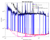
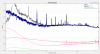
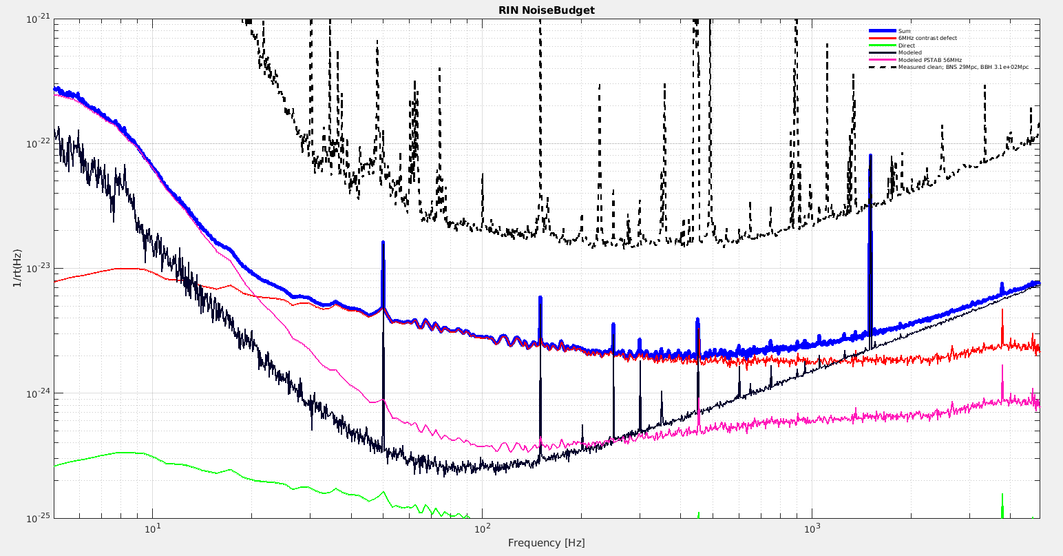
Figure 1 shows the noise budget check from last Sunday, which works well above 100Hz, and which below 100Hz is projecting a noise that is too small. by about a factor 8 at 30Hz.
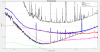
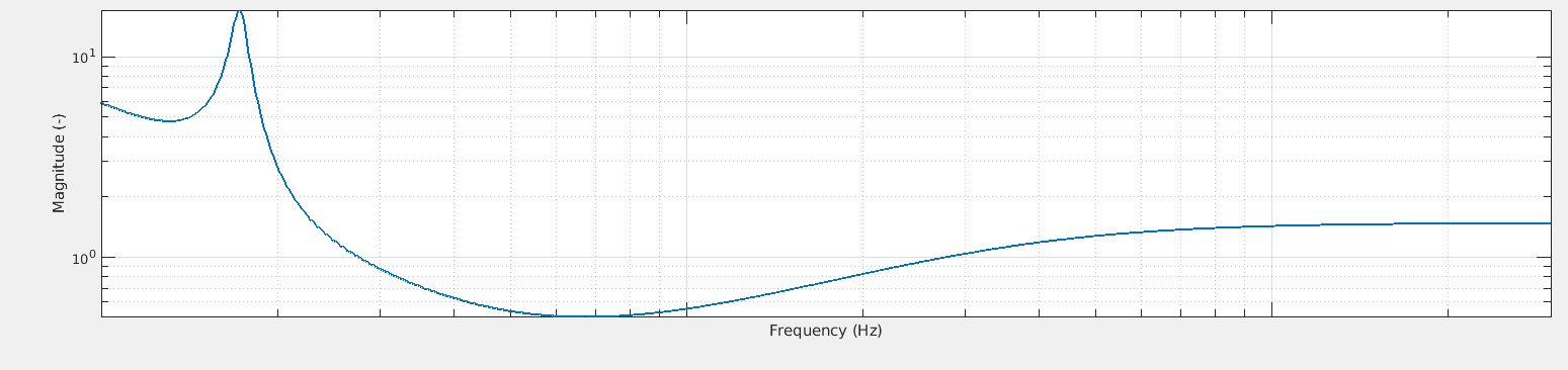
Figure 2 shows a model of PSTAB coupling with an interferometer with a MICH offset of 0.5nm. The figure units are RIN on B1 per RIN of input beam to (without the effect of the DARM loop). The frequency independet part at high frequency is due to the MICH offset, and the low frequency is some other effect that is present in the simulation.
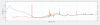
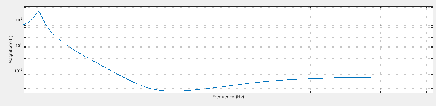
Figure 3 shows this measurement (in red) compared to a scale model (in blue). The curves are in au of DARM per Volt on the PSTAB_PDd_AC_MONIT. The model based on an optical simulation with a MICH offset of 0.5nm is scaled to match the measurement at high frequency, times the model DARM loop transfer function that creates the bumps and notches between 100Hz and 1kHz. I have chosen the model to matche the discrepency with the measurement from March. This means than last Sunday we had a residual offset/RMS on MICH of 0.5nm, while back in March the MICH offset was much larger and had a higher contribution at high frequency compared to low frequency.
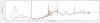
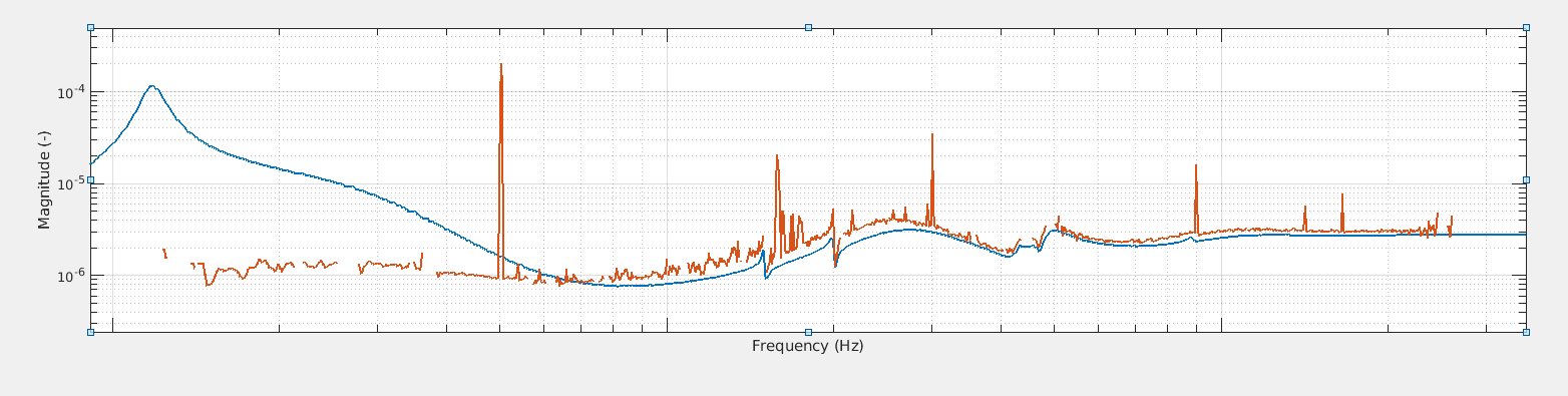
Figure 4, compares the same measurement with a model with 5nm MICH offset, this matches the measurement much better at all frequencies.
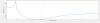
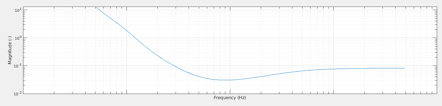
Figure 5 show the 5nm MICH offset model in unites of B1 RIN / input RIN. The coupling at high frequency of ~1 is comparable to the calibrated input RIN to B1 RIN transfer function measurement done back in Mar/Apr

