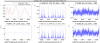
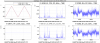
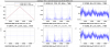
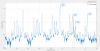
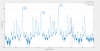
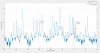
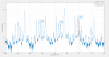
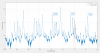
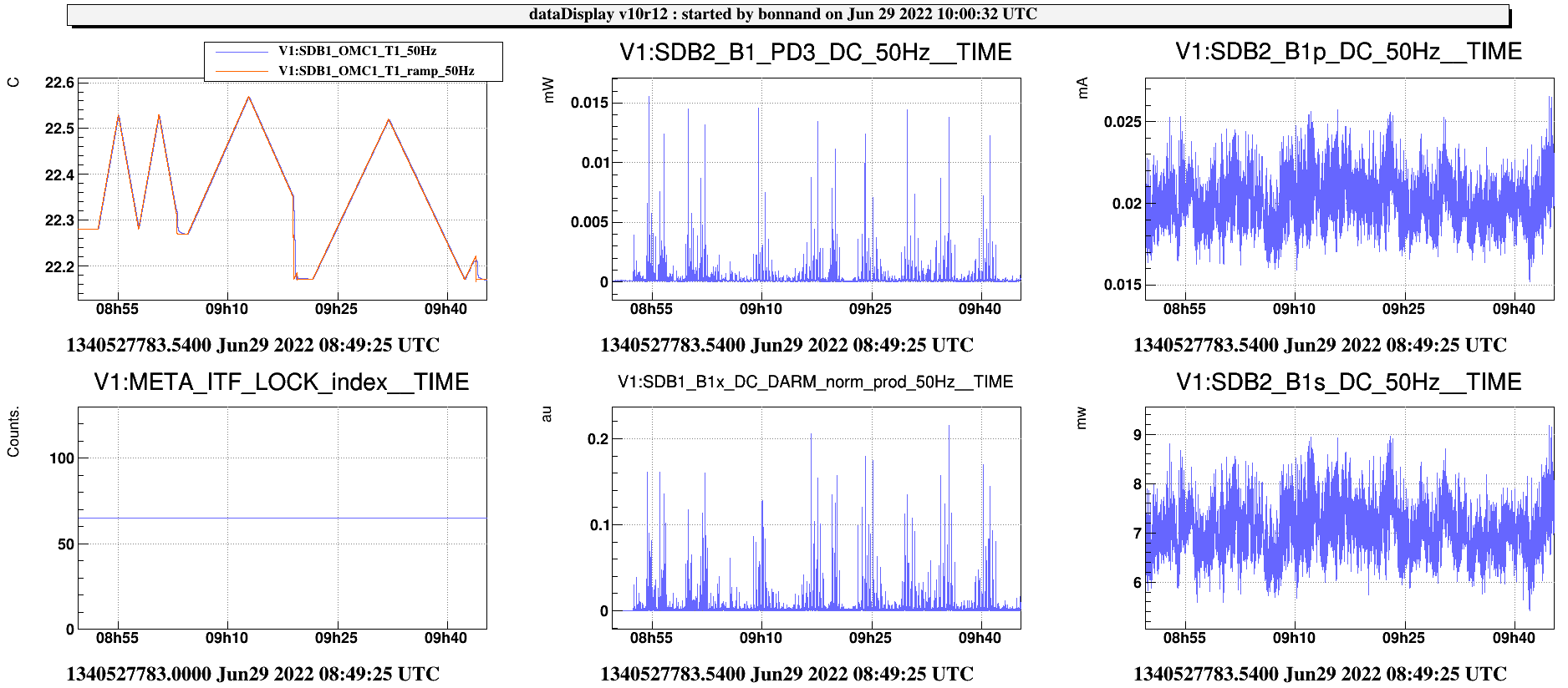
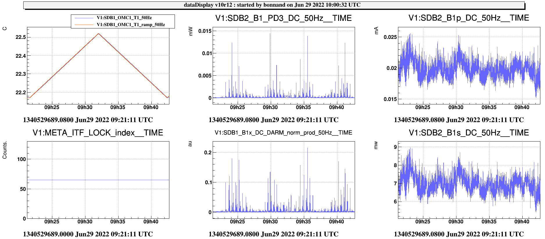
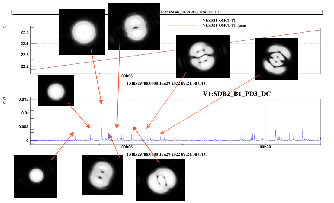
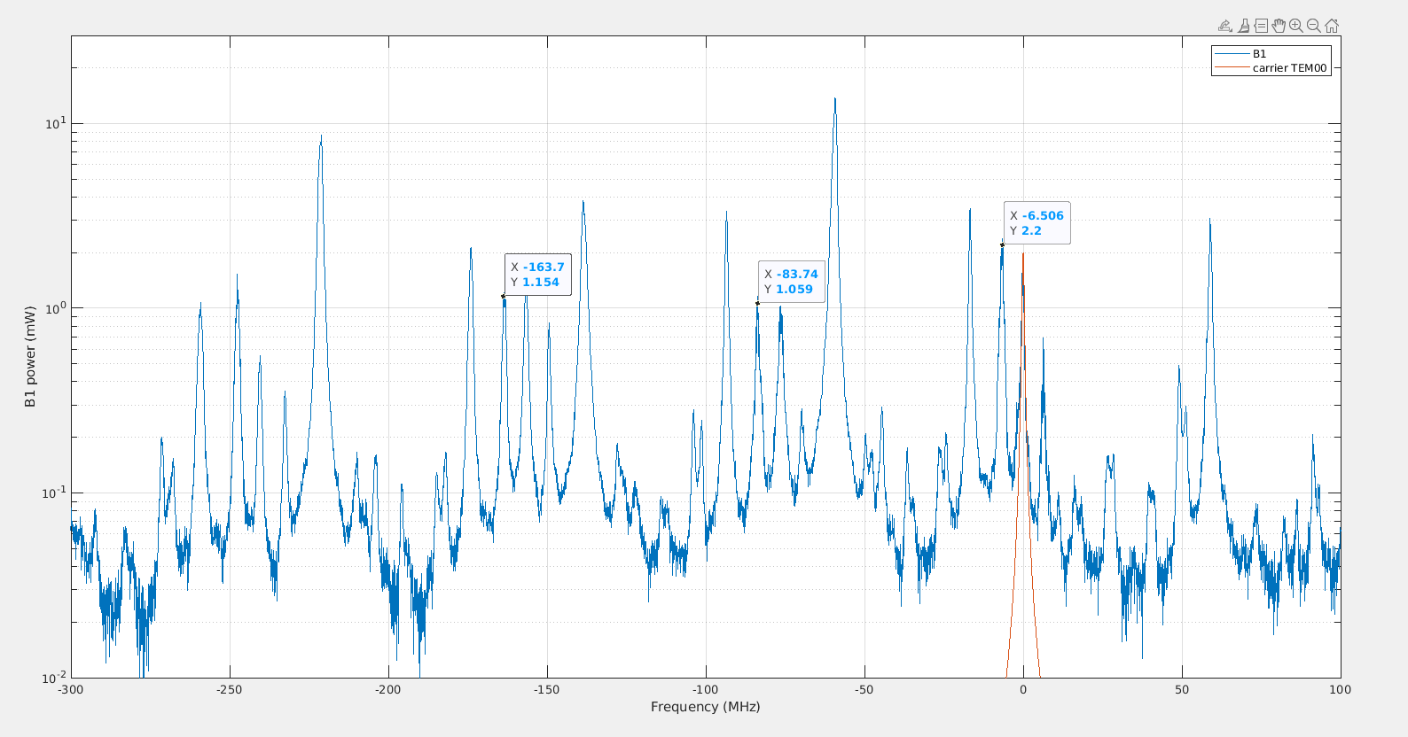
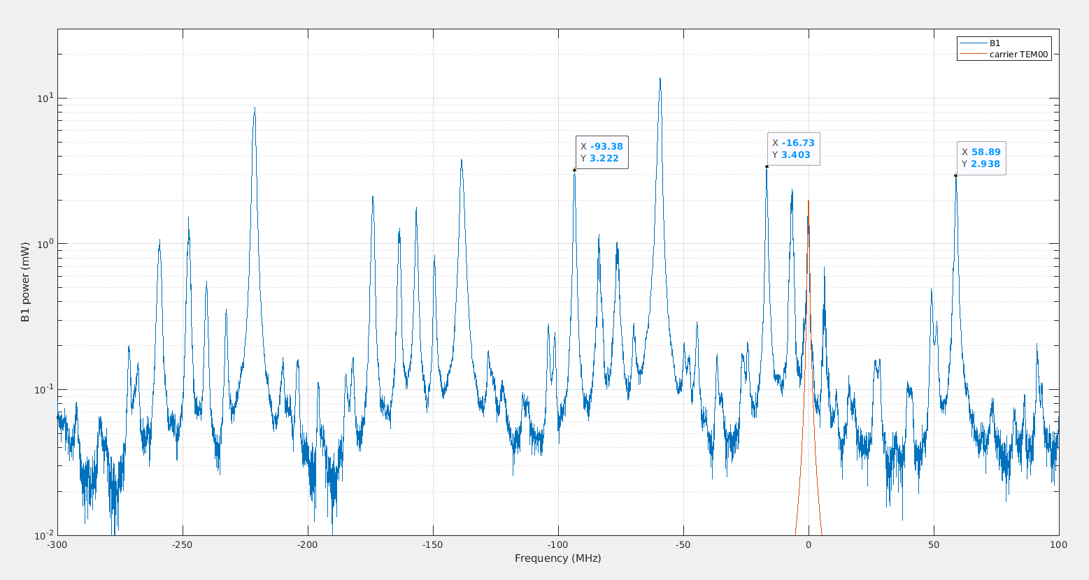
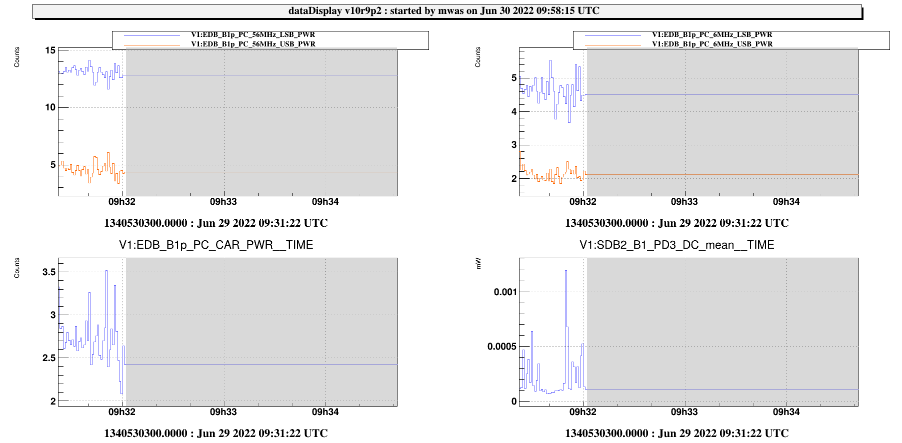
I have looked at the downgoing scan (so it is further away from the steps of the fast scan which will make the relation between the temperature of the OMC, and the temperature of the copper plate measured by the thermistance more linear). Starting from 09:32 UTC.
Also roughly calibrated time into MHz by using the OMC FSR spacing of 864MHz. And then indentified a few modes using the camera image (but I did not check all of them). The power shown in the following figures is B1 PD3 multiplied by 1000, which should be the power transmitted by the OMC, as B1 PD3 looks at a 0.1% pick-off.
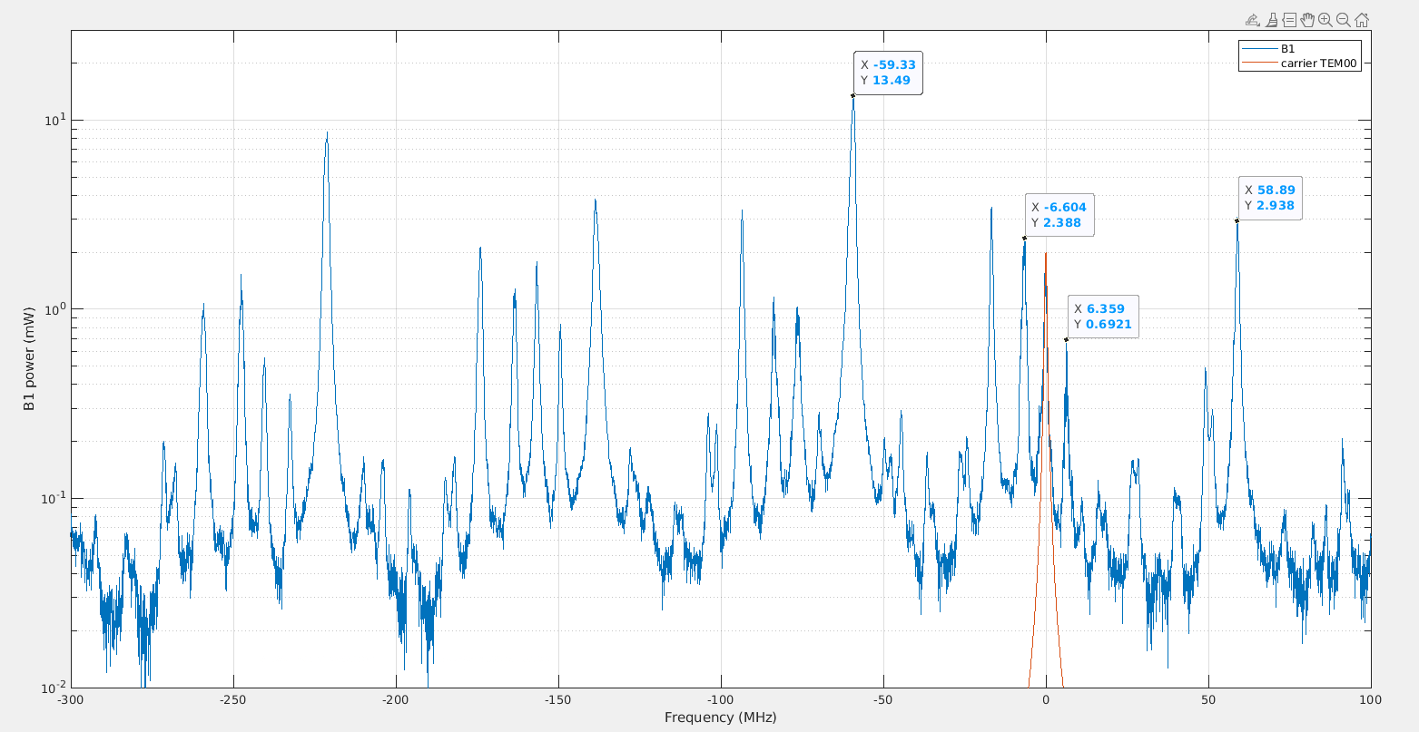
Figure 1 shows the FSR scan around the order 0, 1 and 2 modes. WIth the carrier TEM00 highlighted in red. The tick markes show the 6MHz and 56MHz, LSB and USB.
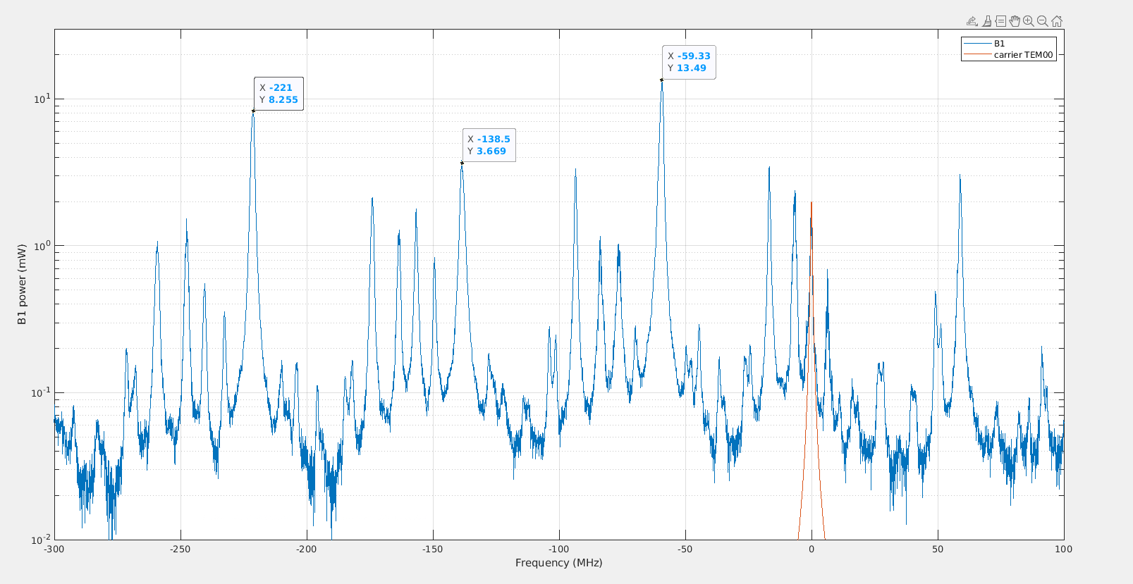
Figure 2 shows the same with tick marks for the 56MHz LSB order 0, 1 and 2 modes.
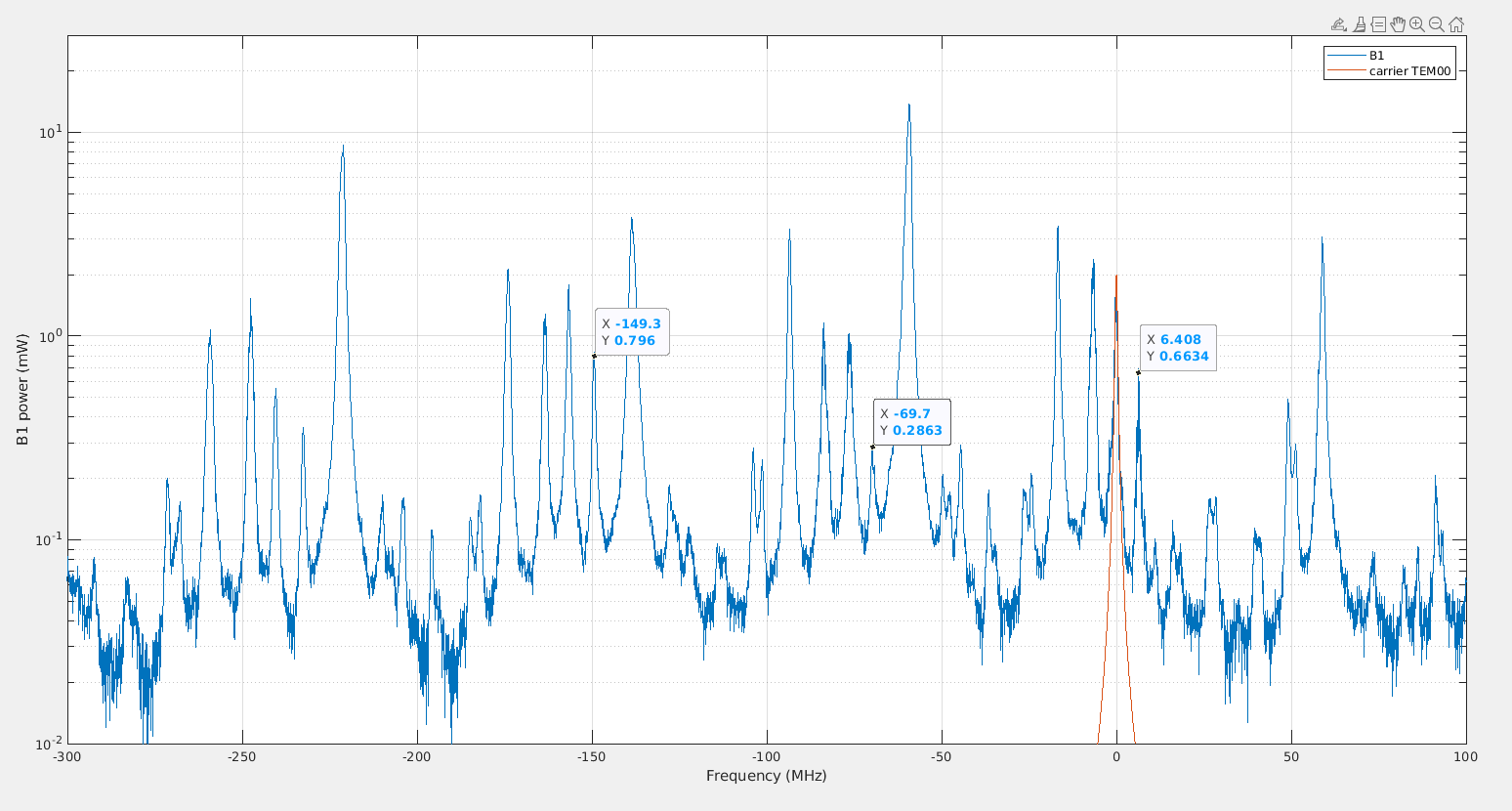
Figure 3 shows the same with tick marks for the 6MHz USB order 0, 1 and 2 modes.
Figure 4 shows the same with tick marks for the 6MHz LSB order 0, 1 and 2 modes.
Figure 5 shows the same with tick marks for the 56MHz USB order 0, 1 and 2 modes.
| Power (mW) | TEM00 | Order 1 | Order 2 | Order 1 / TEM00 | Order 2 / TEM00 |
|---|
| Carrier | 2 | | | | |
| 6MHz LSB | 2.4 | 1.1 | 1.2 | 0.46 | 0.50 |
| 6MHz USB | 0.69 | 0.29 | 0.80 | 0.42 | 1.16 |
| 56MHz LSB | 13.5 | 3.7 | 8.3 | 0.27 | 0.61 |
| 56MHz USB | 2.9 | 3.4 | 3.2 | 1.17 | 1.10 |
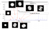
Figure 6 confirms that on the phase camera the LSB (both for 6MHz and 56MHz) has much higher power ( by a factor few) than the USB.
The mode mismatch mode (order 2) is much higher in relative power for the USB (both 6MHz and 56MHz) at ~110% of the TEM00, than for the LSB (both 6MHz and 56MHz) that are at about 50% of the TEM00 opwer.
/users/mwas/OMC/OMC_scan_20220630