Reports 1-1 of 1 Clear search Modify search
AdV-DET (Output mode cleaner)
mwas, gouaty, derossi, spinicelli, menzione - 19:45 Friday 18 February 2022 (54896) Print this report
Output mode cleaner activies: alignment and mode matching checks, scan in dark fringe, attempts to lock at dark fringe

During the first part of the shift, we worked with the ITF in single bounce configuration to check the alignment of the B1 photodiodes, then to check the alignment and mode matching of OMC:

DET MAIN slow shutter automation has issues in single bounce. It fails because it checks the B1p photodiode status immediately after opening the B1p PD2 shutter, before it had time to be updated in the Metatron data that are a few seconds behind. Need to increase the delay of the check to see if it can fix the issue.

Retuned the OMC demodulation phase, was off by 2.5 radian.

Have seen correlation in OMC transmission with B5 quadrant, mainly vertical. Realliged OMC using picomotors, 200 steps in vertical first motor, 100 steps in horizontal first motor and about double that on the second motor (to get a beam shift).

Locked on 56MHz LSB, with 5 times slower scan (0.1 degree of amplitude with 0.1mHz). Observed 0.7mW in transmission of OMC. No light found on B1 PD1/PD2 at first attempt of shutter opening. On second trial B1 PD2 shutter opened. For B1 PD1 we had to try at least ~5 times before it opened. After that could open/close B1 PD1/PD2 shutters without problem.

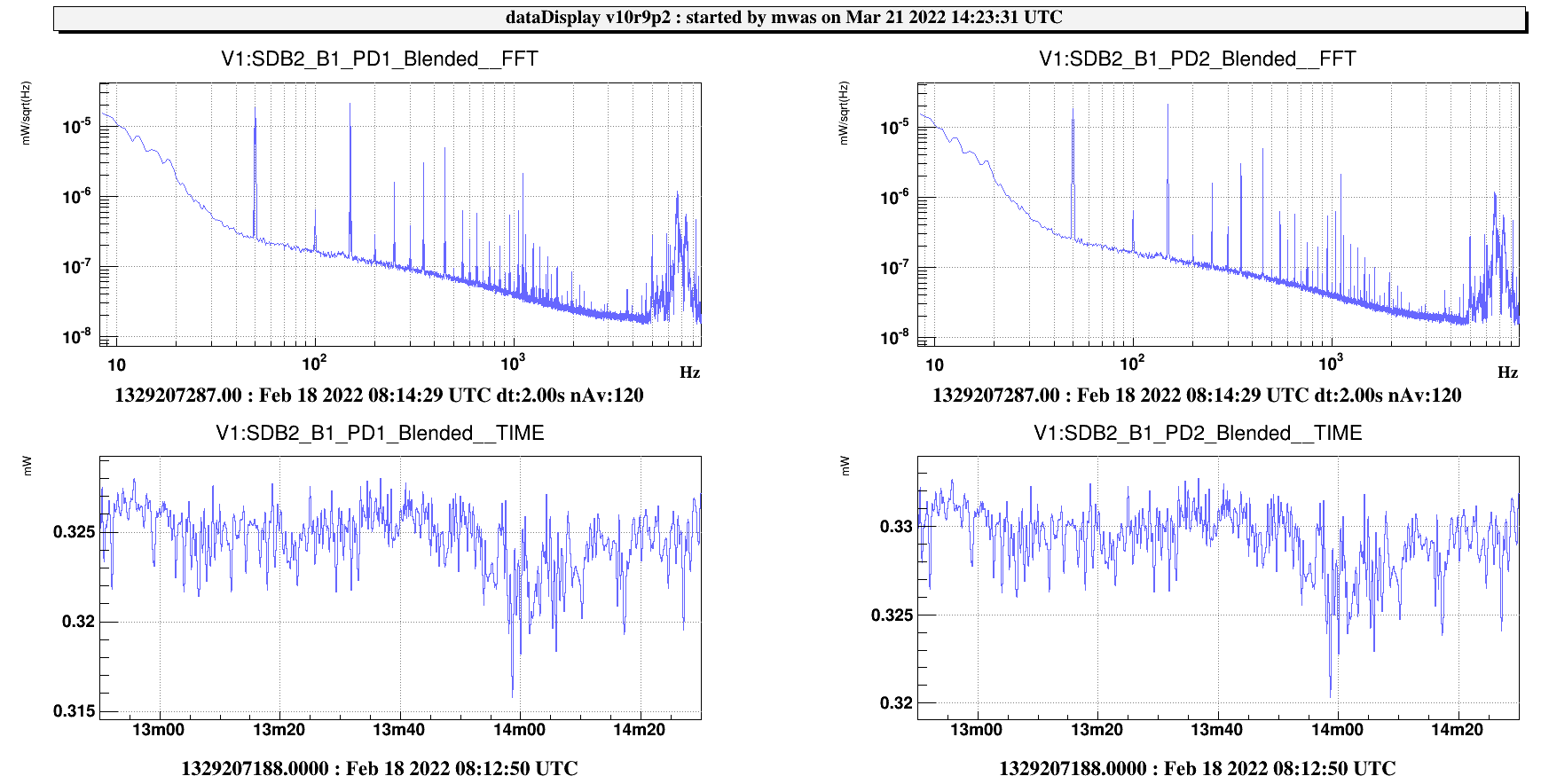
08:12:30 UTC (2min) OMC locked on LSB 56MHz with no action. Maybe could analyze 56MHz RIN later with these data.

Checking B1 PD1/PD2 alignment by moving SDB1 in TY by ±500urad. Beam on B1 camera moves by ±0.8mm. At opposite edges of motion each photodiode losses 1% (one edge for PD2 and the other for PD1).
Moving in TX by ±100urad. Moving by ±0.2mm no clear impact on B1 PD1/PD2. More power on B1s PD1.
Realigned B1s PD1 using picomotor in reflection of OMC on SDB1.

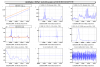
08:34:30 - Up-going scan 0.1 degree with 1mHz frequency:
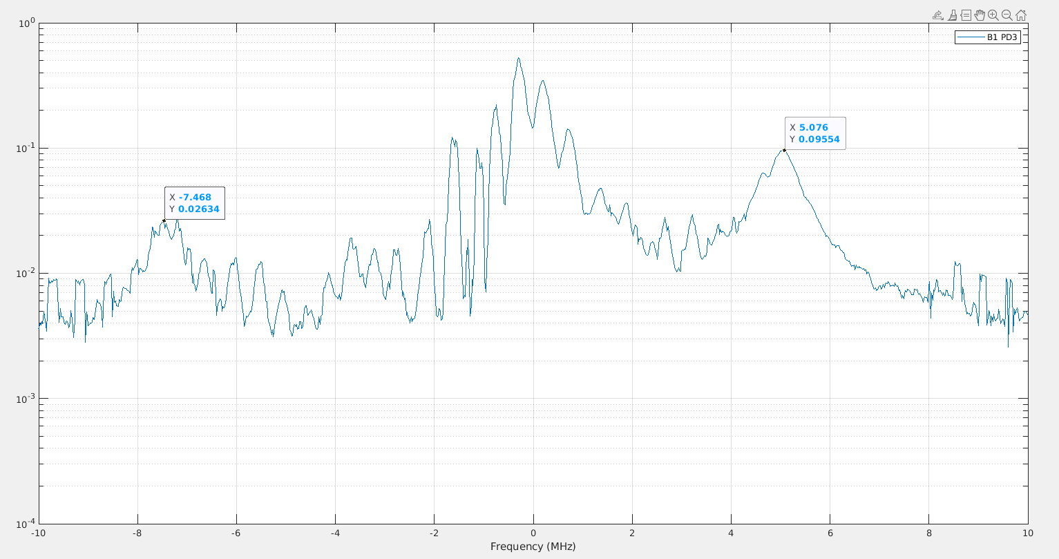
0.65uW - LSB 56MHz TEM00
0.105mW - carrier TEM00
0.65uW - USB 56MHz
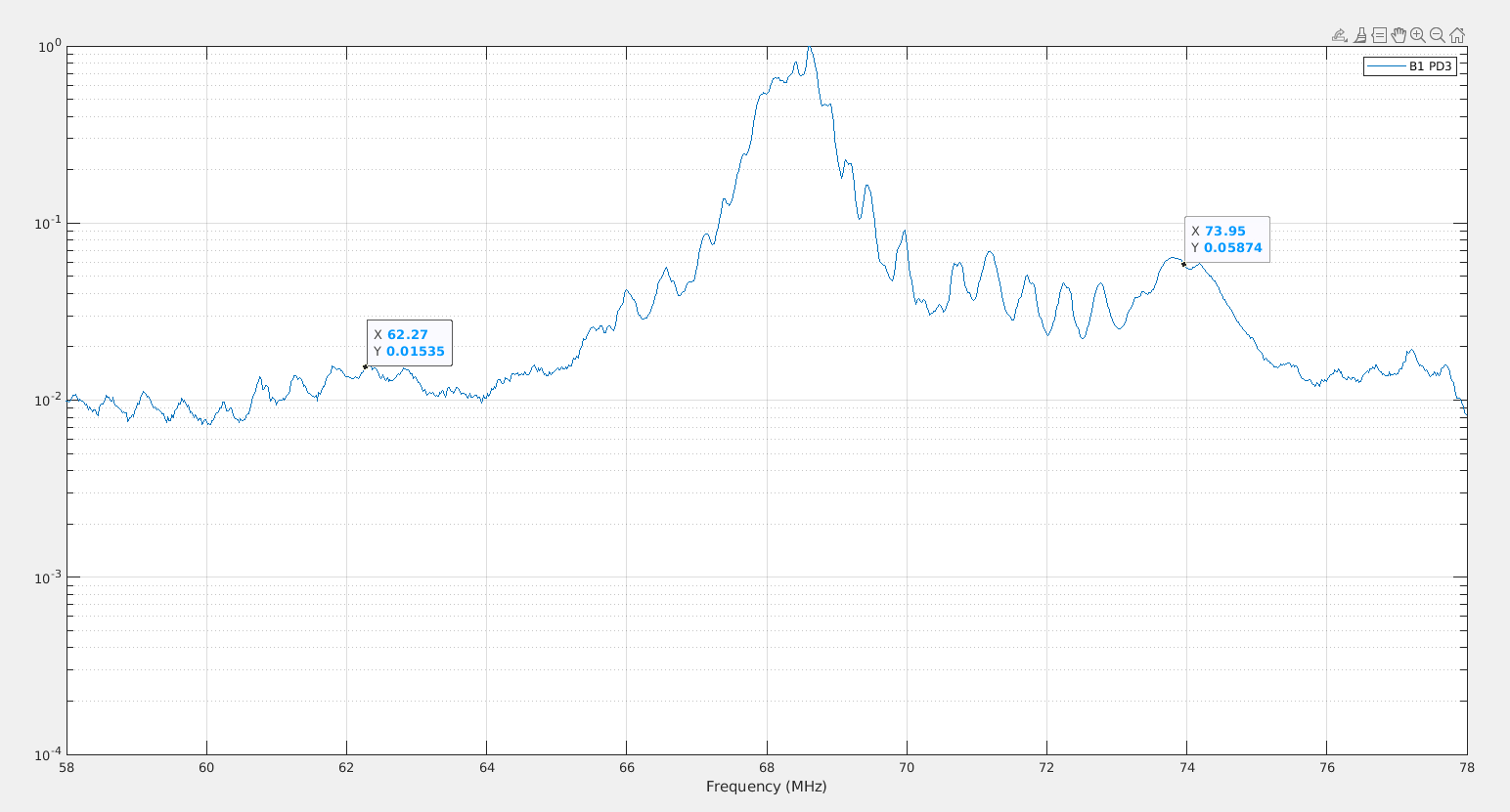
0.95uW - carrier order 1 mode vertical
carrier order 2 mode saturated B1 PD1/PD2 and closed fast shutter
0.02mW on B1 PD1/PD2 for order 2 mode of USB 56MHz

08:43 down going scan with B1 PD1/PD2 closed:
0.05uW on order 2 mode of USB 56MHz
5.5uW on carrier order 2 mode
08:47 end of scan

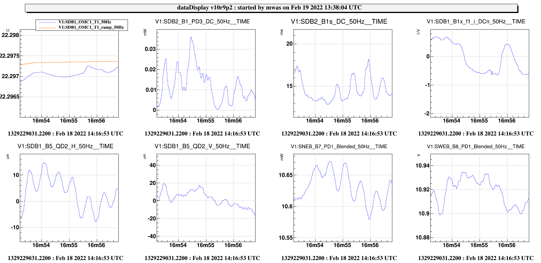
08:53 UTC (3min) OMC locked on carrier light with no action. Correlation with SDB1 TX still visible, around ±1%, for ±50um on B5 QD2 V.

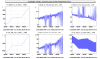
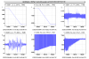
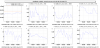
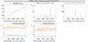
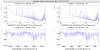
Adjusted SDB1 in Z by ~2mm (see Fig.1). Realligned a little bit the OMC with picomotors in H. Transmitted power clearly improved by ~5%.

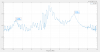
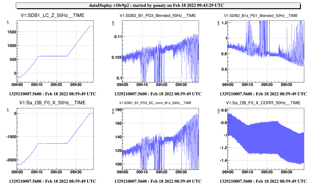
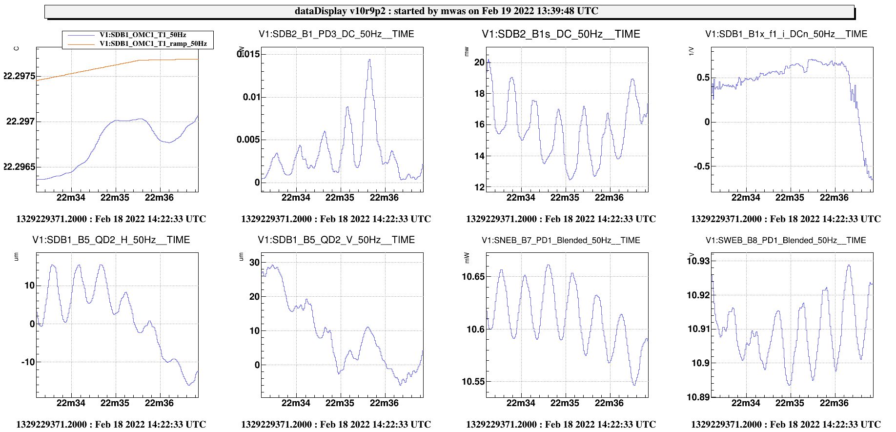
09:44:40 (3min) scan after mode-matching and alignment (see Fig.2):
0.11mW on TEM00
0.001mW on order 1
0.0027mW on order 2

We improved the mode matching but the order 2 mode is still at 2.5% of TEM00. As we did not want to spend too much time on mode matching tuning (considering that the input beam will be better matched to the FP cavities next week) we decided to stop the mode matching tuning here and try to lock the OMC at dark fringe.

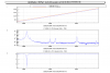
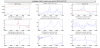
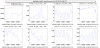
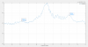
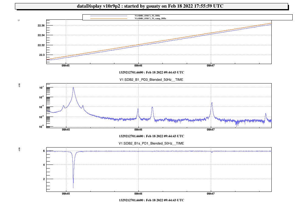
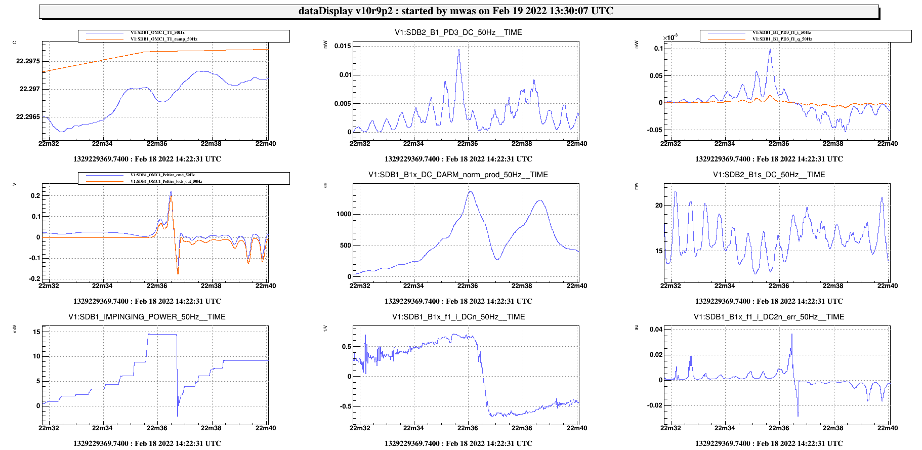
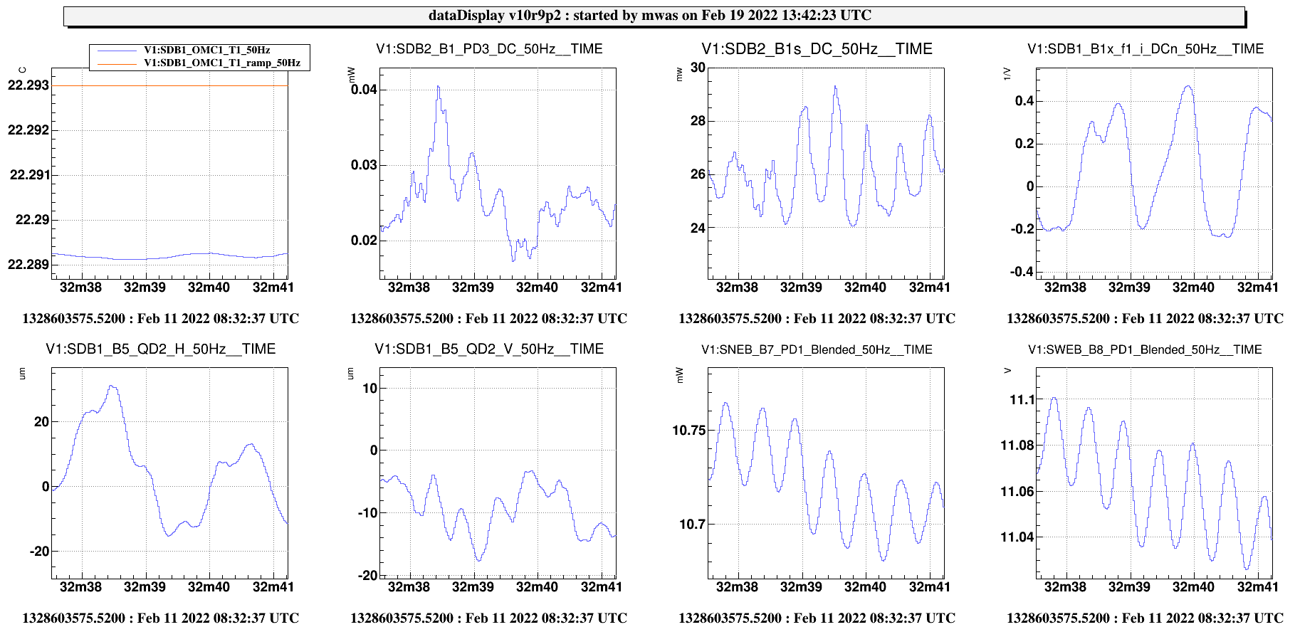
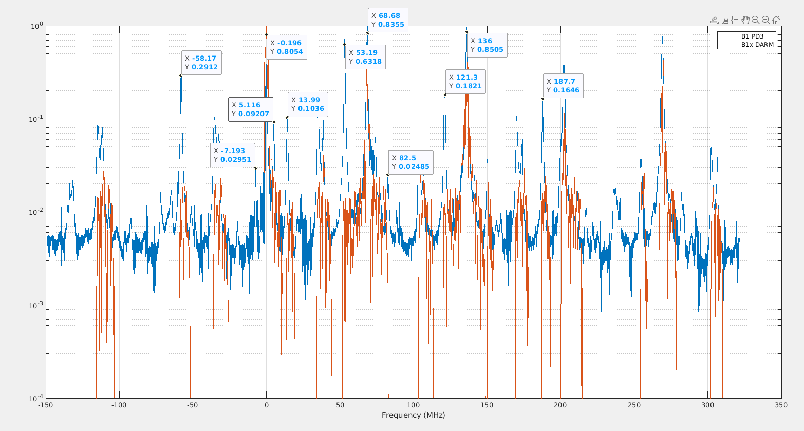
After Piernicola and Camilla restored a stable lock at dark fringe, we put a dark fringe offset LSC_DARM_SET=-0.2 and we scanned the OMC in these conditions (amplitude 0.12 deg, frequency 1 mHz), starting from 13h05m30 (see Fig.3). A fine analysis of this scan will be performed later, below is what we observed on the fly:

TEM00 of SB (56 LSB ?) at 6.5 mW.

Carrier TEM00 at 11 mW.

TEM00 of SB (56 USB?) at 15 mW.

Carrier first order mode at 20 mW.

Carrier second order mode at 20 mW.

Carrier third order mode at 8 mW.

Carrier fourth order mode at 16 mW.

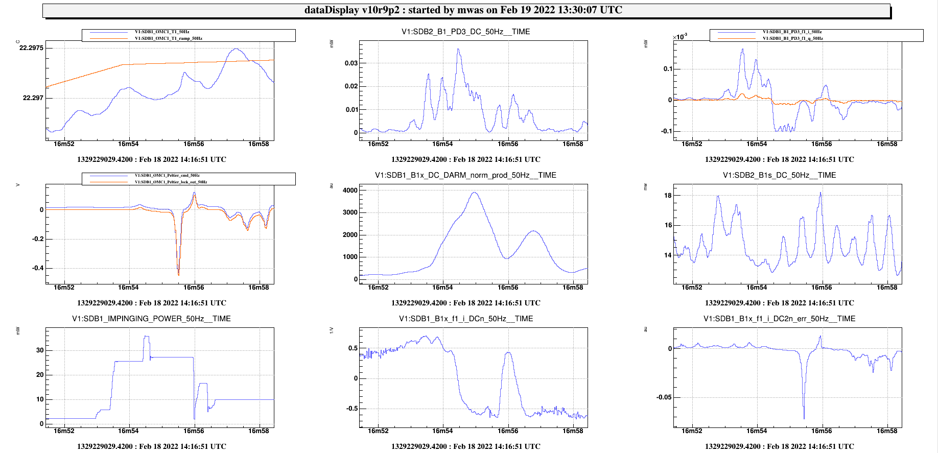
We started a down-going scan but the ITF unlocked at 13h16m36 due to a large power on B1s (reaching the threshold of 43 mW that triggered the closing of SDB1 fast shutter).

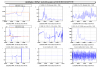
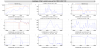
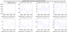
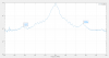
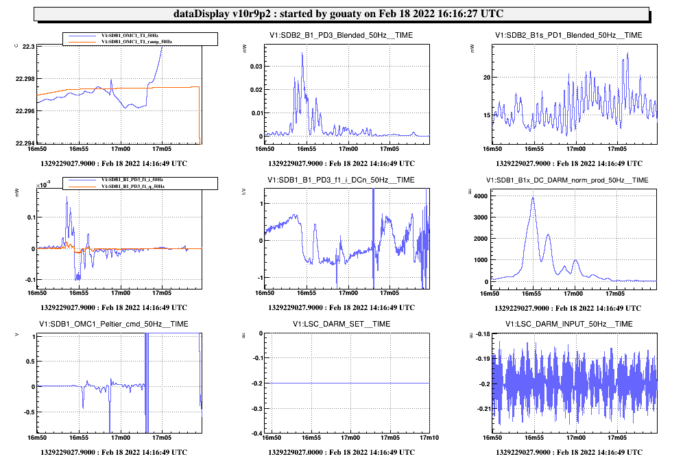
After the ITF was relocked in dark fringe, we tried to the lock OMC but failed (Fig.4). A first attempt of OMC lock is shown in Fig.5 with the dark fringe offset put at -0.2. The power on the carrier TEM00 was fluctuating around 20 mW, which should have been OK. The scan parameters were amplitude=0.12 deg and frequency = 0.0003 Hz.

Another failed attempt of OMC lock with an increased dark fringe offset at -0.3 is shown in Fig.6.

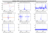
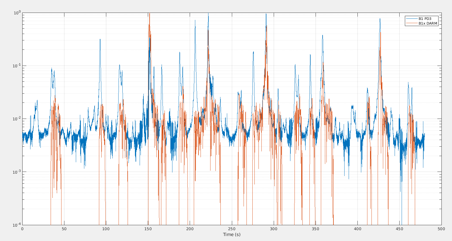
Then we stopped trying to lock the OMC and tried to scan it around the carrier TEM00. Fig.7 shows the crossing of the carrier TEM00. What is strange is that the power seems to be reduced (no more than 7 mW in transmission) while the DARM offset is still at -0.3.

Further analysis has to be performed to better understand the causes of this two failed OMC lock attempts.

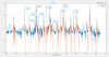
At the end of the shift, upon request from the commissioning coordinator, we brought bench the SDB1 bench at its initial longitudinal position in order to not risk any side effect on the Hartmann beam. Fig.8 shows that while the SDB1 bench is moving along Z, the B1p position on the camera is changing by ~0.8 mm. Note that the SDB1 drift control was not engaged during that time, which is probably the reason for this large alignment drift not compensated the alignment of SDB1.

Next time we will work on the OMC, we should start by checking the alignment and the mode matching again.

Images attached to this report
Comments to this report:
mwas - 15:01 Saturday 19 February 2022 (54906) Print this report

Figure 1 and 2 show two of the OMC lock attempts. The main issues is the large spikes present on the DC2n (DC squared normalized) error signal. This is the signal used in loop, as it has a larger linear range, but has a gain that depends on the dark fringe offset power. Here will going through the OMC transmission peak the power is fluctuating by a factor ~10. Too much for this error signal to work.

Figure 3 and 4 shows that the OMC transmission is maximal whenever the ~2Hz oscillation in B7 power is high. It doesn't appear to be an alignment problem, as the transmitted power is not clearly related to the beam position on SDB1 B5 QD2 (although the 2Hz oscillation is also clearly visible there).

Figure 5 shows the situation last week when the OMC was locked on CARM null. The 2Hz oscillation in B7/B8 was also present with a similar amplitude. It was a bit smaller on the SDB1 B5 QD1 signal, but it is less clear as there was an ~0.5Hz oscillation with larger amplitude (+/-30um), hiding the smaller (+/-10um) 2Hz oscillation.

So it is unclear to me why the dark fringe power was oscillating yesterday, but it is clearly the reason for the failed locks. Finding the origin of this oscillation could solve the problem. Otherwise locking the OMC using the DCn (single normalized) error signal would be more robust to this issue (but requires a slower OMC temperature ramp to achieve a lock).


Images attached to this comment
mwas - 16:03 Saturday 19 February 2022 (54907) Print this report

Figure 1 and 2 show the same part of the upgoing OMC temperature scan. In blue is the transmitted power, and in red is the transmitted power demodulated at the DARM length dithering frequency (73Hz?), both are normalized to 1 at the max transmission in the scan. Fig 1 is with time on the axis, and Fig 2 is the same data with time roughly calibrated into frequency compared to the carrier TEM00.

One can notice that the lower sideband TEM00 of 56MHz has half the power othe upper TEM00. And the lower 6MHz TEM00 has 1/4 of the power of the upper 6MHz TEM00. So there is a clear unbalance in the sidebands, and it is in the same direction for both sidebands. This unbalance is clearly visible in the B1p phase camera (but the convention between LSB and USB is reversed). With also a factor 2 for the 56MHz sidebands, and between a factor 4 for the 6MHz. So the OMC scan agrees with the relative sideband powers measured with the phase camera, and also with the power of the 56MHz relative to the power of the 6MHz.

Looking at the not normalized powers, there is 2mW in 6MHz USB, 0.5mW in 6MHz LSB. While from simple simulations (VIR-1225B-19) 10mW in total for LSB+USB was expected for 40W input power, and a high modulation index of 0.25. While for the 56MHz there is 6mW in the LSB, 12mW in the USB, so 18mW in total. While 600mW is expected in theory (for a modulation index of 0.25 that is likely much higher than what is actually used). Note that this is an underestimate as these side-bands are clearly not perfectly mode matched with the OMC, so the actual powers can be easily a factor 2 higher. But for the 56MHz the power seems at least a factor few smaller than expected for a perfect interferometer.

The modes (TEM00, order 1, order 2, etc) are separated by about 68MHz.

  • So the LSB 56MHz order 1 mode is at ~12MHz, and USB 56MHz order 1 mode is at 124MHz. Both of them are roughly 1/3 of the corresponding TEM00 power.
  • The LSB 56MHz order 2 mode is at ~80MHz  and the USB 56MHz order 2 mode is at ~192MHz. The LSB has 8.5% of the TEM00 power in the order 2 mode, while the USB has 26% of the TEM00 power in the order 2 mode. It is surprising that the LSB has 2 times less power even though it seems much better mode matched with the OMC (which had been measured to have a mode mis-match to the input beam of ~3%).

Unfortunately the B1 camera image is stored in the raw data at 0.1Hz (although it is available online at ~1Hz). So the numerology above cannot be checked in images. Would it be possible to store the B1 camera image in the raw full data at the same rate as available online?


Images attached to this comment
mwas - 12:18 Tuesday 01 March 2022 (55030) Print this report

Below I try to get some information on the 6MHz sideband from the OMC scan in CARM null.

Figure 1 shows the TEM00. With the 6MHz on the right (LSB on the phase camera), 4 times taller than the 6MHz on the left.

Figure 2 shows the order 1 mode, again the 6MHz on the right has 4 times more power than on the left, and has half the power of TEM00. So a strong misalignment, that is not a good overlap between the two Michelson arms which lead to an order 1 mode in the destructive interference. The order 1 mode on the left is not much higher than the backrgound wings of the carrier light.

Figure 3 shows the order 2 mode. The 6MHz on the right is maybe a factor 2 higher than on the left, but the one on the left is not much higher than the carrier background wings, so it is hard to judge. The order 2 6MHz on the right has maybe 15% of the 6MHz TEM00 power.

Images attached to this comment
mwas - 15:34 Monday 21 March 2022 (55244) Print this report

Forgot to analyze the data from a month ago when the OMC was locked in single on the 56MHz sideband with B1 PD1/PD2 open.

Figure 1 show the spectrum and DC power on the photodiodes. I corresponds to a power fluctuation of 5e-7 1/rtHz at 100Hz which should correspond to the modulation relative amplitude modulation noise, while during O3 with the full interferometer we had measured 7.5e-7 1/rtHz (VIR-1225B-19). There is a 50% discrepency to be understood.

In any case, the signal seems clear, and the impact of installing the RAM servo could be easily checked after it is installed, by locking again the OMC in single bounce on the 56MHz sideband. The RAM servo should reduce this noise by factor ~10. Checking other sidebands will be more difficult.

Images attached to this comment
Search Help
×

Warning

Error

The present report has been modified outside this window. Please check for its integrity in the main page.

Refreshing this page will move this report into drafts.

×