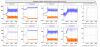
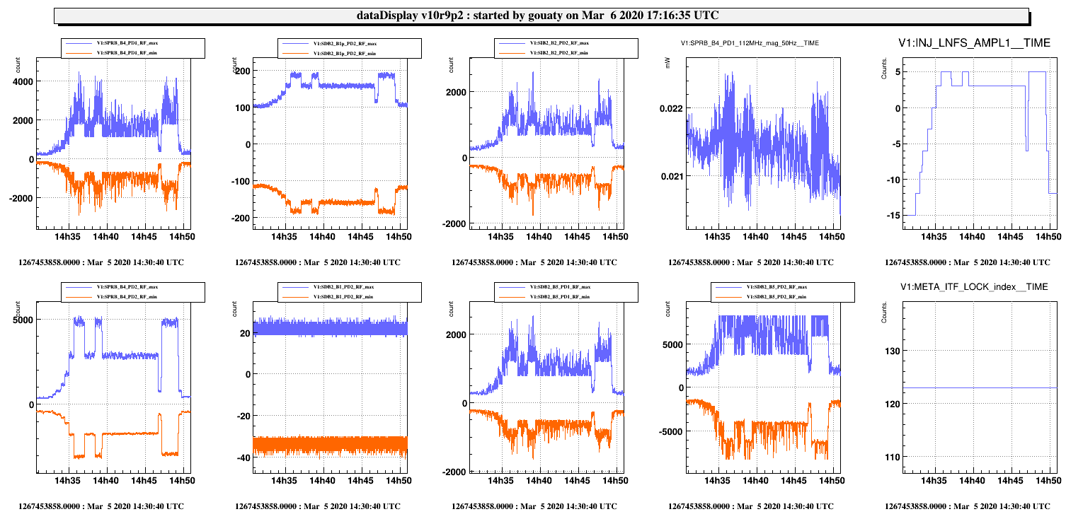
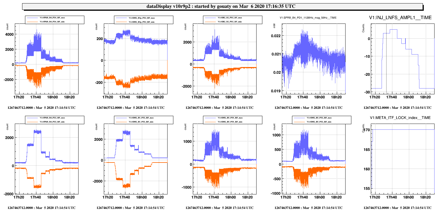
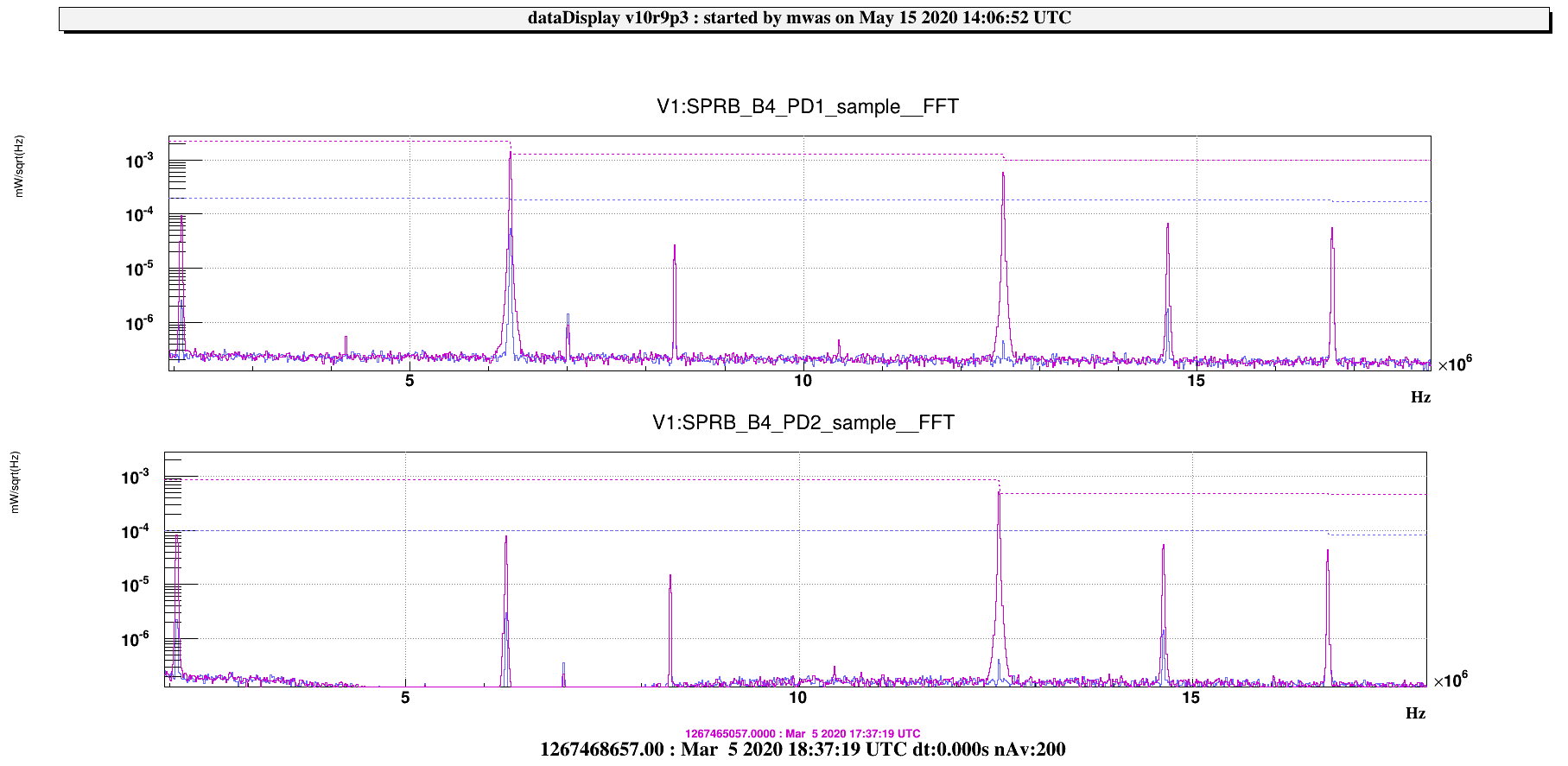
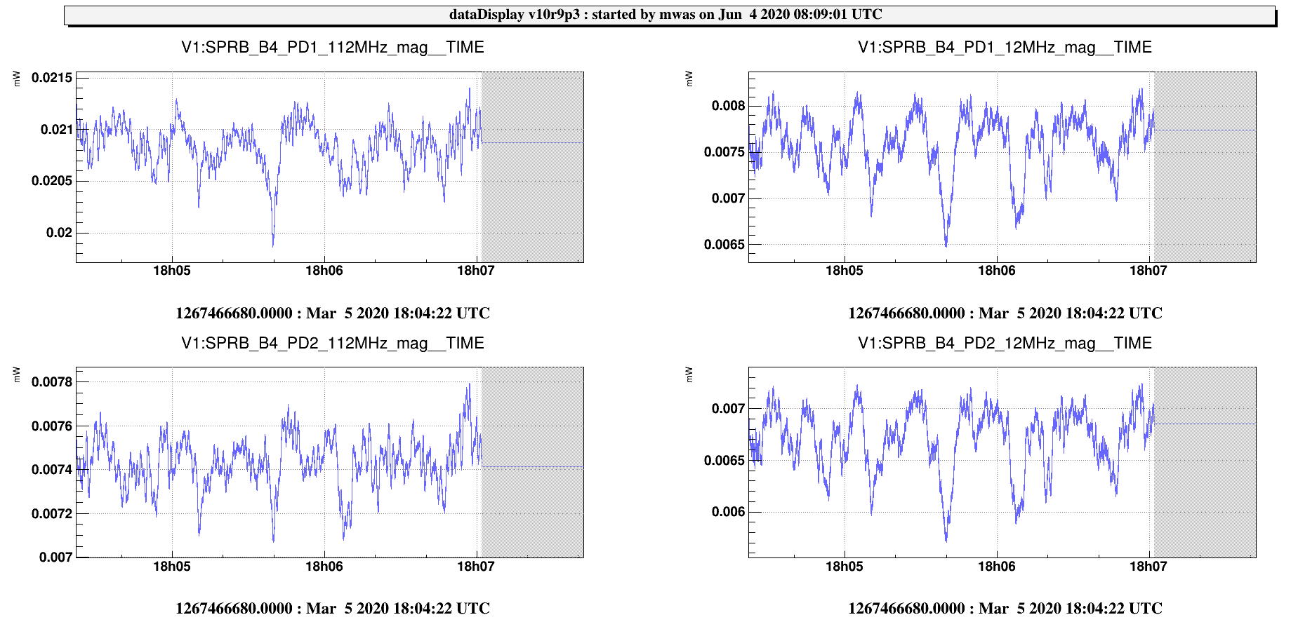
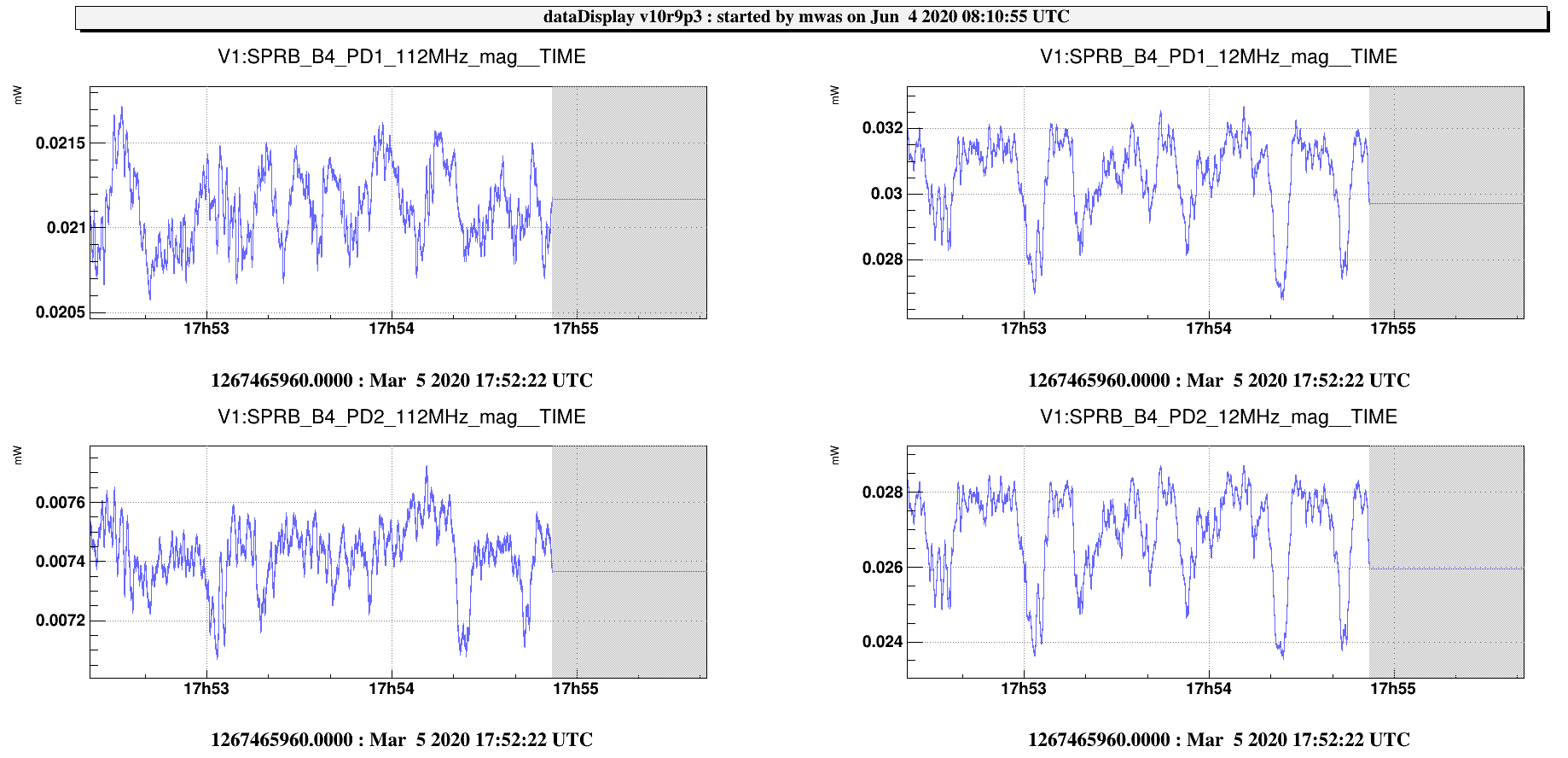
The data with the increased modulation depth of the 6MHz in LN3 to 3dB (purple lines in the figures) can be compared to the normal conditions with -28dB modulation of the 6MHz (blue lines).
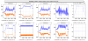
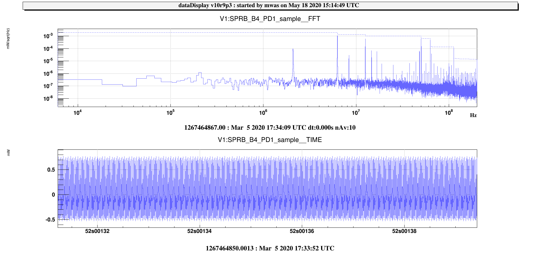
In the figures we compare two photodiodes B4 PD1 and PD2, which see the same power. The differences are that PD2 has an analog notch at 6MHz, which reduces the line by a factor ~20. Also itis a 3mm diameter photodiode compared to 2mm for PD1, which means that above ~20MHz the response of the PD2 photodiode is a factor 2 smaller than of the PD1 photodiode due to the photodiode capacitance.
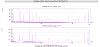
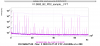
Figure 1 shows the broadband RF spectrum, the dominant lines are the 56MHz+/-6MHz, 12MHz and 6MHz. On PD2 the 56MHz+/-6MHz lines are a factor 2 lower due to the PD size. The 12MHz line is about the same in both. And the 6MHz is a factor 20 lower in PD2 due to the notch.
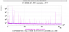
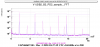
Figure 2 zoom into the region between 1MHz and 20MHz. Comparing purple and blue the 12MHz line is increased by a factor 1000 as expected from the 31dB increase in modulation. The 6MHz, 2MHz and 14MHz are increased by a factor 30 in both photodiodes, also expected from the 31dB increase in modulation. The 14MHz and 2MHz are the beat notes between the 8MHz and 6MHz, in principle the height should be half way in between on a log scale between the 12MHz and the 16MHz, hower they are almost equal to the 16MHz, a factor 3 smaller than expected. The probable reason is that the overlap between the 6MHz and 8MHz beam shape is poor, of the order of 50% in amplitude (so ~30% in power). The only sign of non linearity in PD1 on that figure is the small line 4MHz.
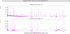
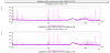
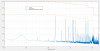
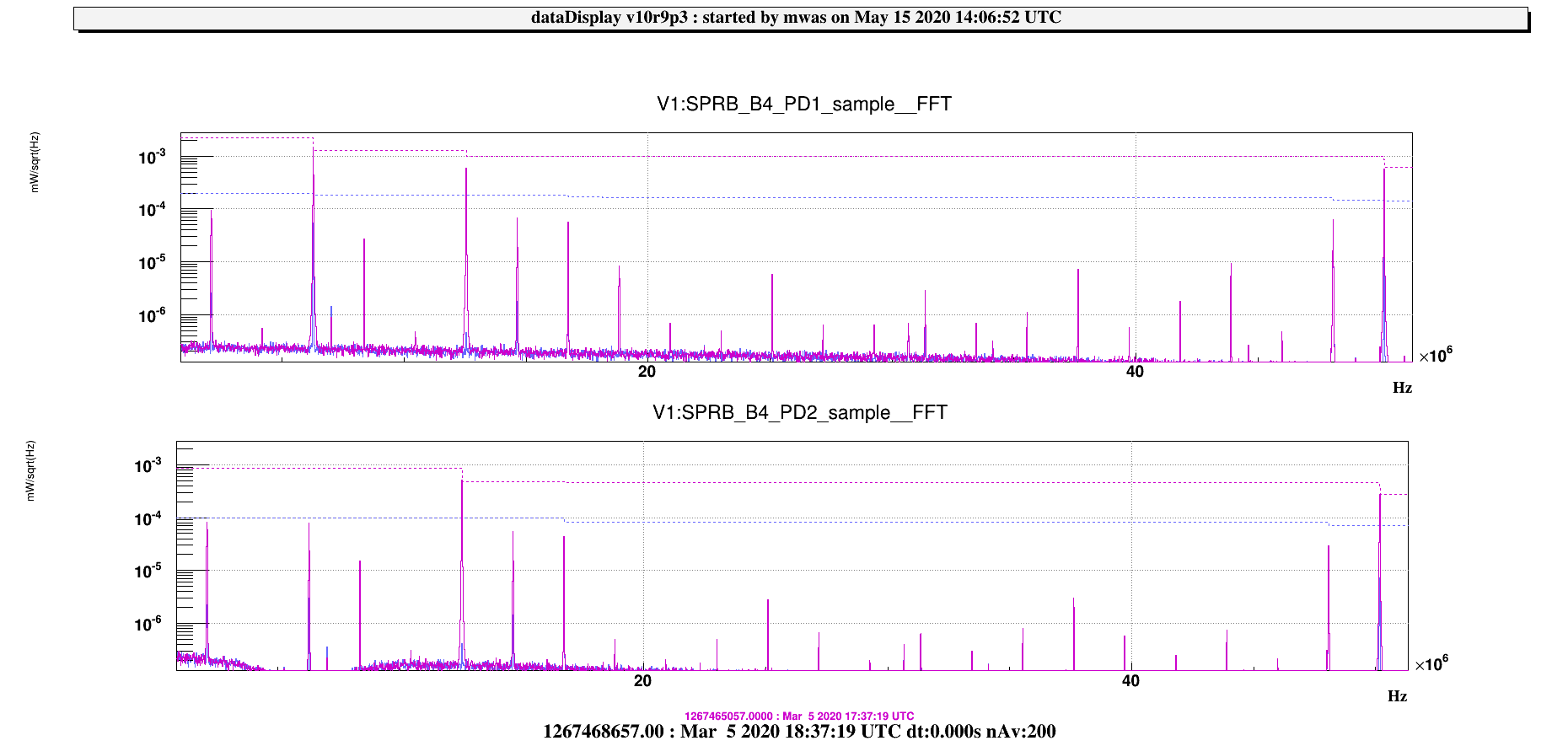
Figure 3 zoom between 2MHz and 50MHz, there are several lines which are much higher in PD1 than in PD2, the 3*6MHz line is a factor ~20 higher, and the 7*6MHz is a factor 10 higher. The 5*6MHz line is a factor 4 higher. The 4*6MHz and 6*6MHz line are a factor 2 higher in PD1, but that is expected due to the larger size of PD2. An additional 2dB of 6MHz modulation was causing PD1 to saturate, so this increase in odd harmonics of the 6Mhz shows the beginning of the distorsion in the signal due to non linearities close to saturation, not however that these harmonics are over 2 orders of magnitude smaller than the 6MHz itself.
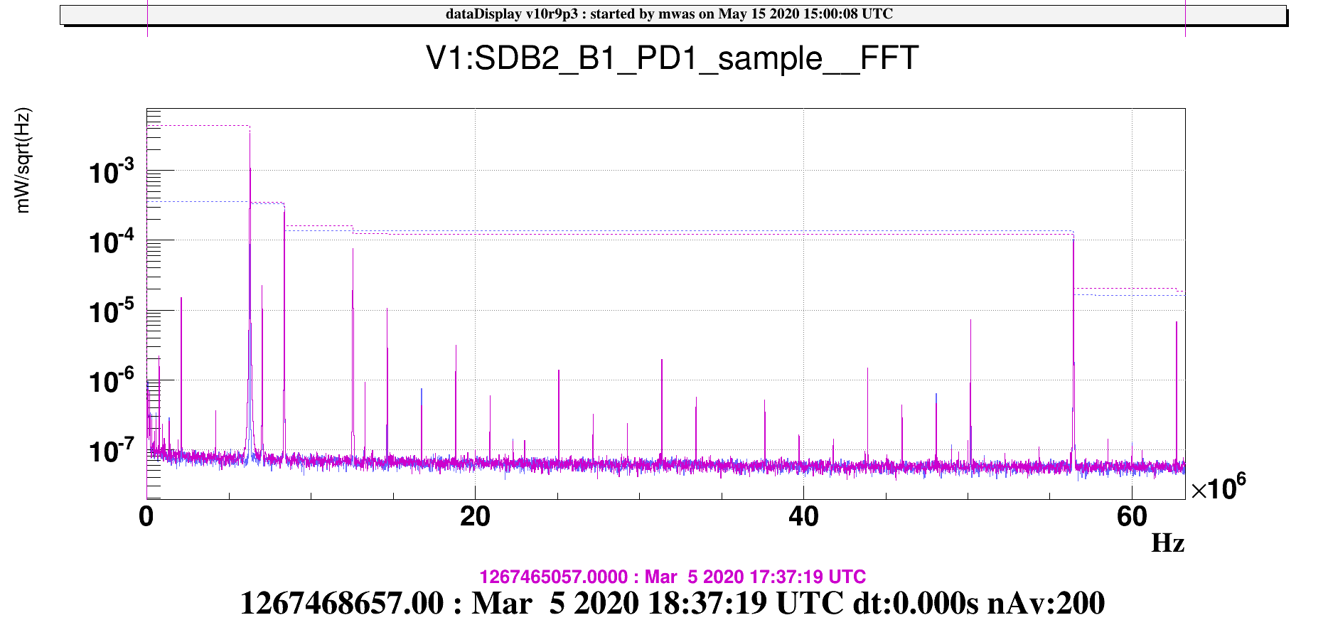
2mW RMS of RF spectrum appears to be a limit of this photodiode design. It consistent with LNA (ABA-52563) data sheet saturating at 1V RMS, assuming there is no other gain factor than the 2.592 into the DAQ. The notch at 6MHz on PD2 is able to reduce this RMS by a factor 2 to ~1mW. The next three contributors in PD1 are the 12MHz, 50MHz and 62MHz which each contribute ~0.7mW RMS, for a total of 1.2mW RMS (in PD2 the 50MHz and 62Mhz are smaller due to the PD size).
The biggest limitation to increasing the modulation depth is the 12MHz as increasing the modulation to 13dB would increase its amplitude by a factor 10 to 7mW RMS. So a notch at 12MHz would be definitely needed to reduce the amplitude to 0.4mW RMS. An already notched 6MHz would increase by a factor 3 to 0.3mW RMS. Notching the 50MHz and 62MHz, is impossible without removing also the 56MHz. So these would increase each of these sidebands 2.1mW RMS, for a total of 3mW RMS. The LNA planned for O4 (PHA-13LN+) starts to distort signals for a 7dB higher signal according to the data sheet. So should be able to handle 4.5mW RMS with the same distorsion as seen here for PD1 with 2mW RMS. So a notch at 6MHz and 12MHz with the new LNA should be able to handle 13dB of 6MHz modulation with a factor 1.5 of margin with regard to the start of distorsions. However, the power increase from 25W to 40W is equal to that margin of 1.5. So keeping the power at 40mW on these photodiodes may be needed, by dumping some of the power on SPRB on a beam dump.
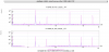
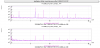
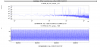
Figure 4 shows the situation for B1. The 6MHz saturates the photodiode with 4mW RMS. The new high finesse OMC design will reduce the 6MHz power on B1 by a factor 10. Also signal recycling will reduce the amount of 6MHz reaching the photodiode by another factor 8, as the 6MHz is not resonant in the SRC. This gives in total a decrease by a factor 80 in power, or a factor 9 in the 6MHz beat with the carrier. If the 6MHz modulation depth is increased to 13dB, the 6MHz beat would increase by a factor 3/9, and the 12MHz would increase by a factor 10/80. In total this would give 1.3mW RMS on the photodiode for the 6MHz, and 0.04mW RMS for the 12MHz. The filtering of the 56MHz will not change for O4, but the power of the sidebands might increase by a factor 5. This would bring the 56MHz to 0.3mW RMS. In conclusion notches should not be necessary for the B1 photodiode in O4, but we might consider it as a precaution for the 6MHz, if it doesn't have an impact on the squeezing signal planned for O4 at ~4MHz.
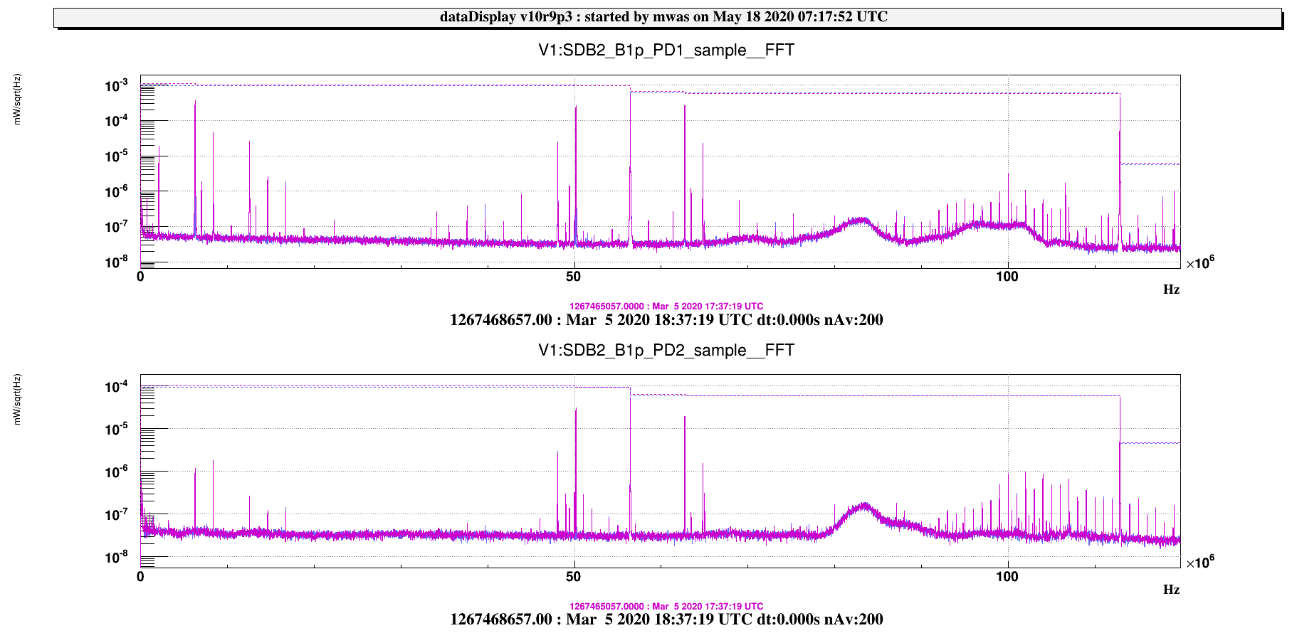
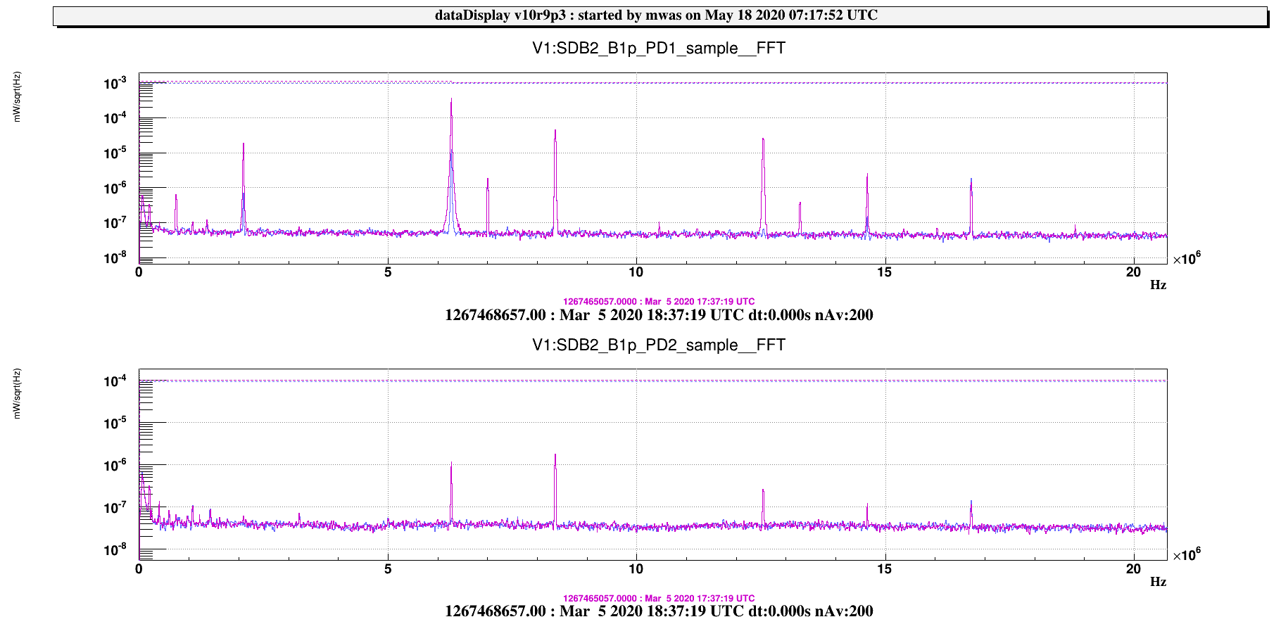
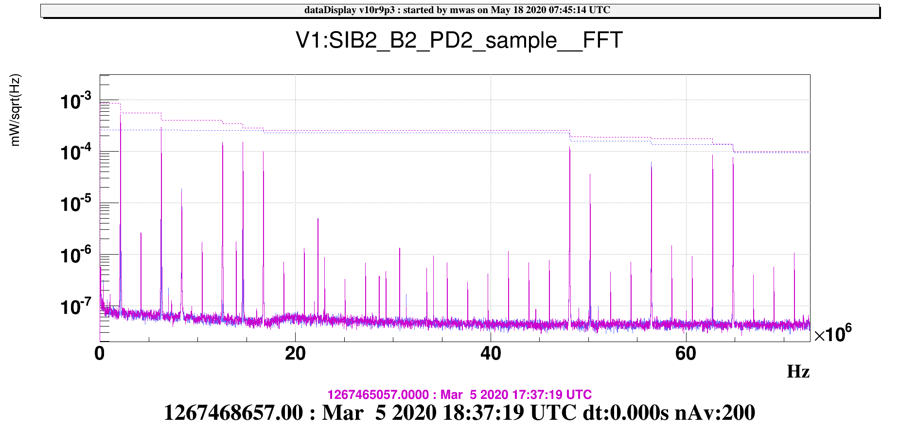
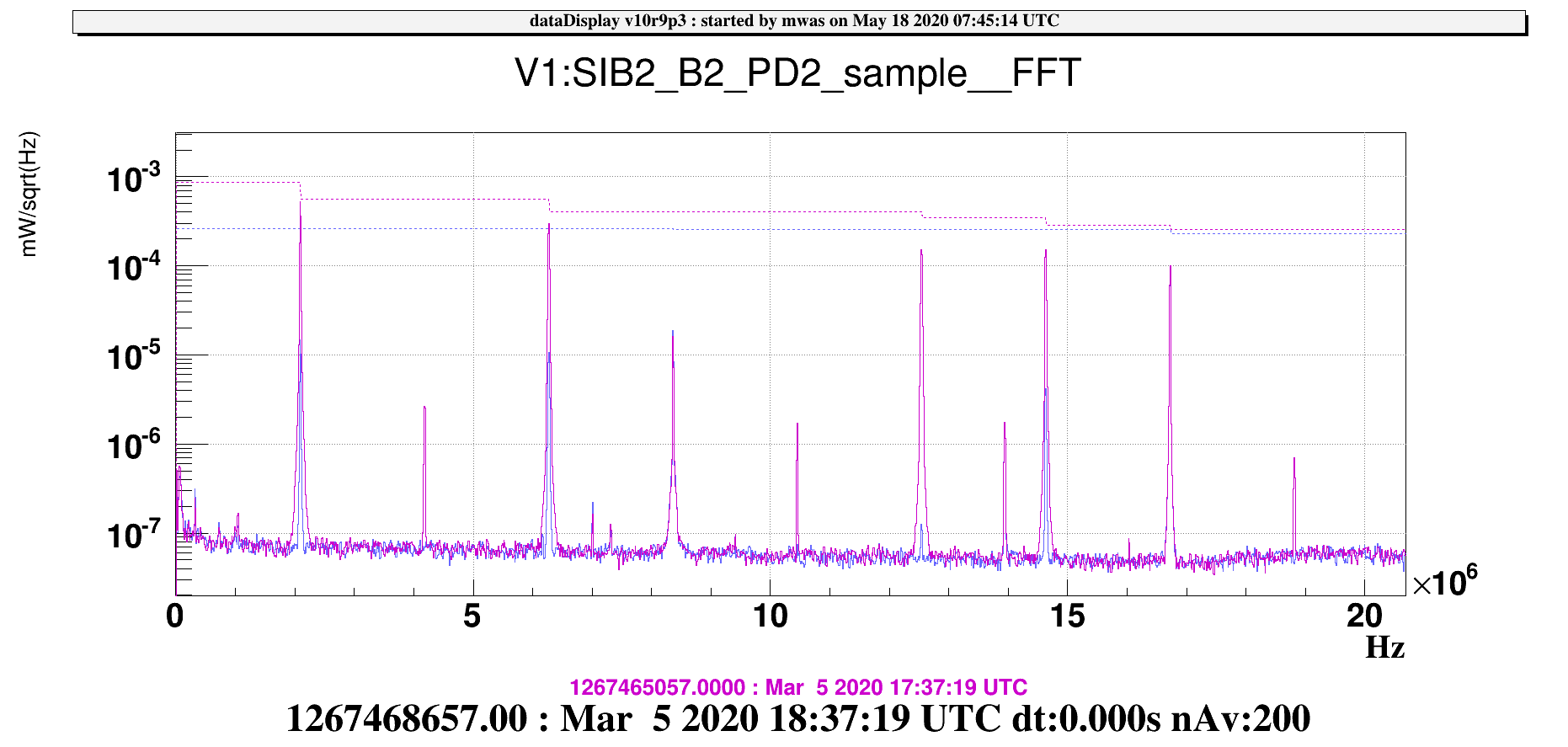
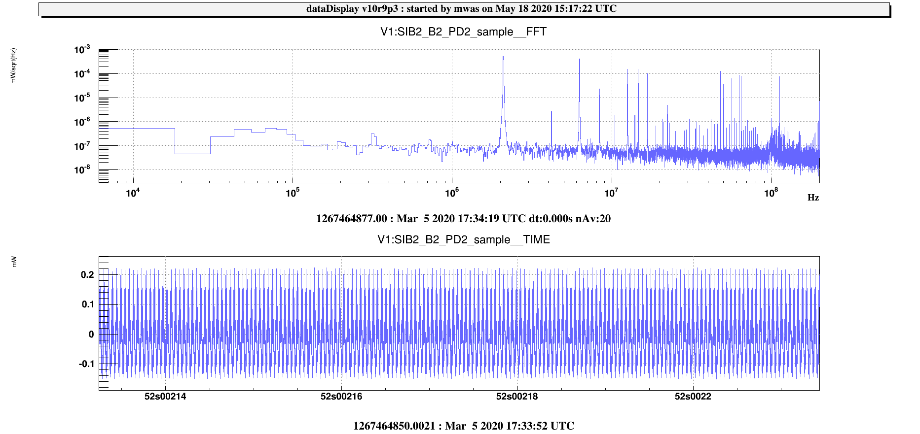
Analysis remains to be done for B1p and B2.


