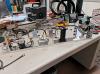
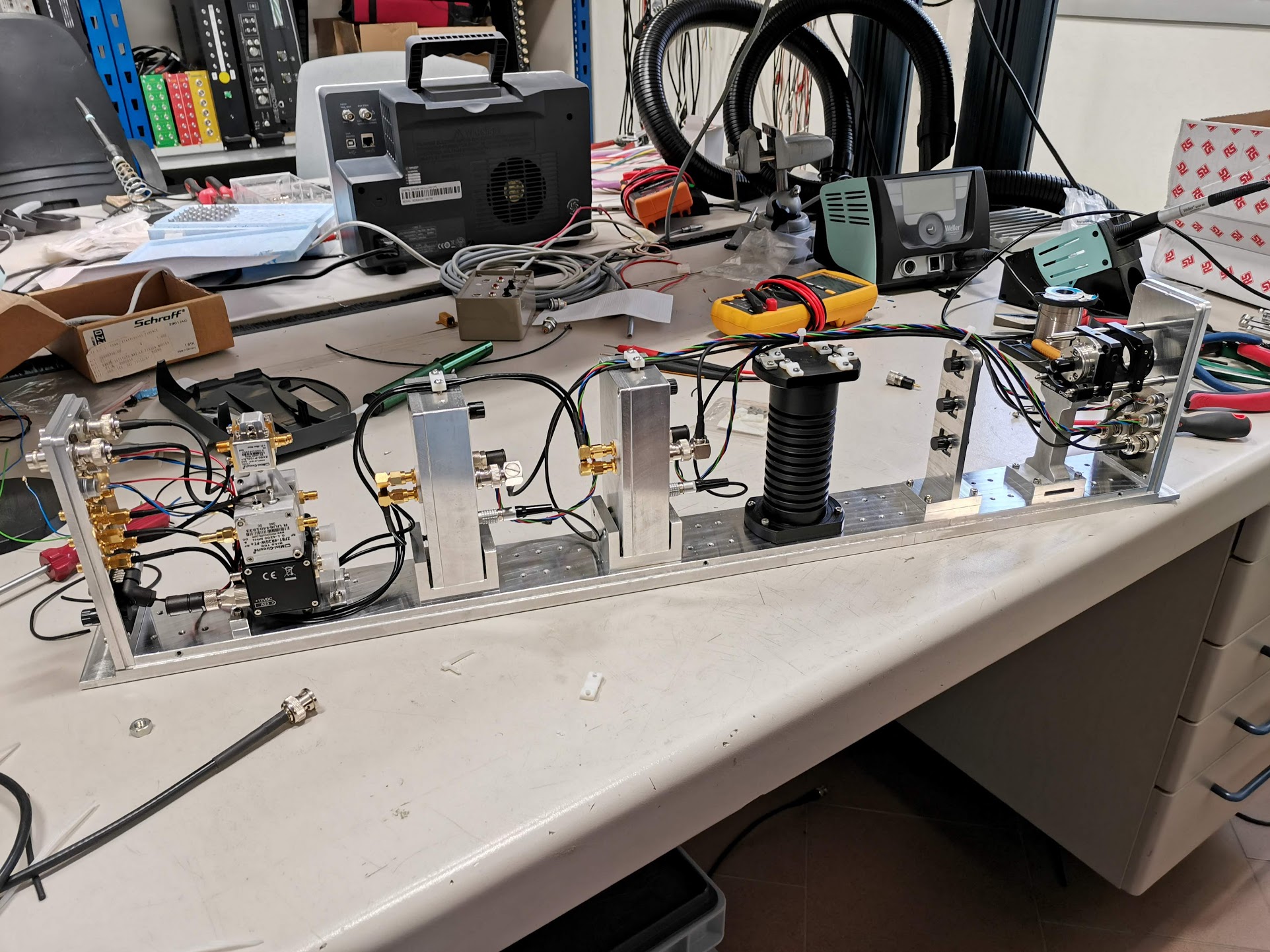
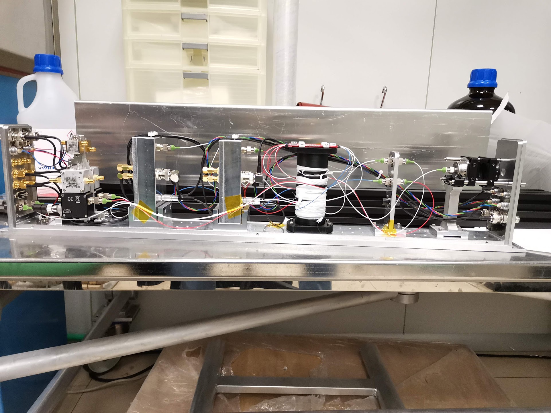
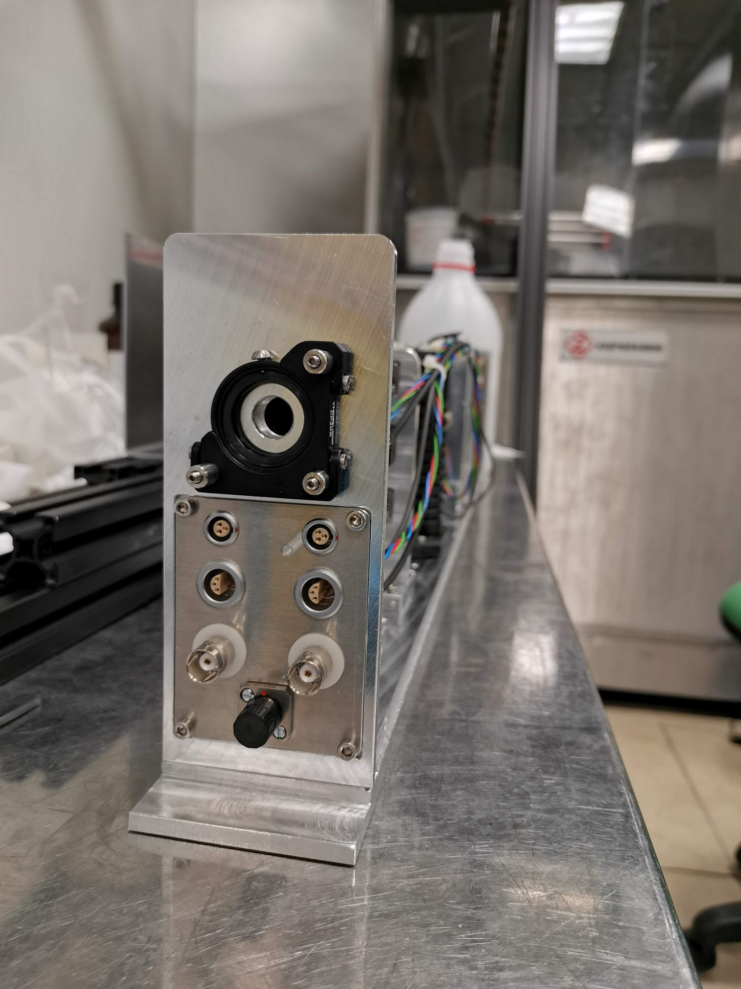
The photodiode box of the PLL is quite ready/ Figure 1 shows the open box just after the cabling and figure 2 shows the box with all the optical fiber installed.
Description of the box:
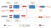
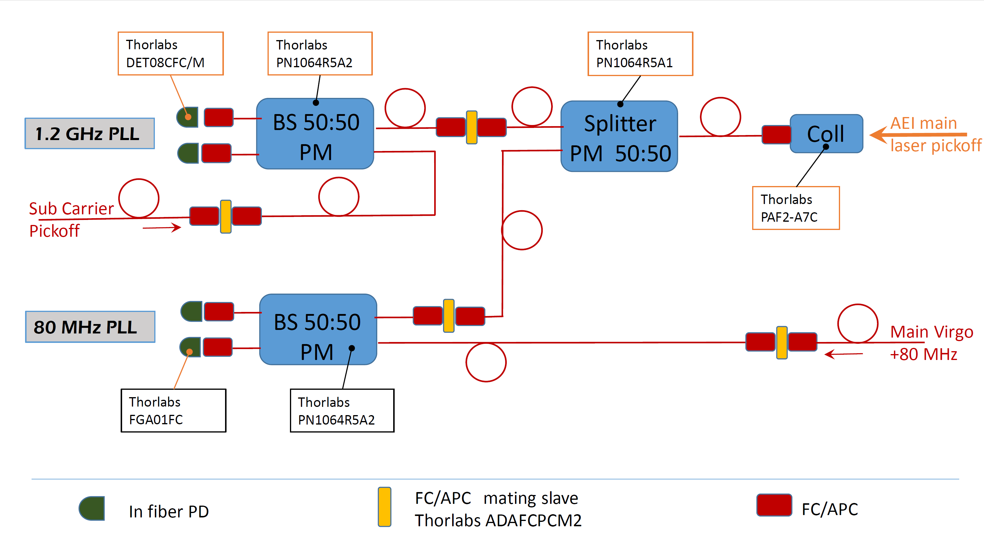
The box contains all the optical component for the PLLs of the SC (scheme in figure 3).
- The SQZ Main Laser enters in the box in free space and is fibered coupled with a collimator. Outside the box, before the hole for the laser input is plaed a diaphragm that helps for the centering.
- Once entered the SQZ Main laser is splitted in two parts with a fibered splitter (Thorlabs PN1064R5A1 ) each of the line is used for a different PLL
- Main PLL: the SQZ Main Laser and the PSL Pick off are superposed with a fibered beam splitter ( Thorlabs: PN1064R5A2 ). The PSL pick off arrives from INJ room to the DET room with a PM 50m optical fiber. The two photodiodes used for the beat note detection are two pig tailed photodiode (Thorlabs FGA01FC), whereas the Photodiode amplifiers are the same used during O3 with minor modifications)
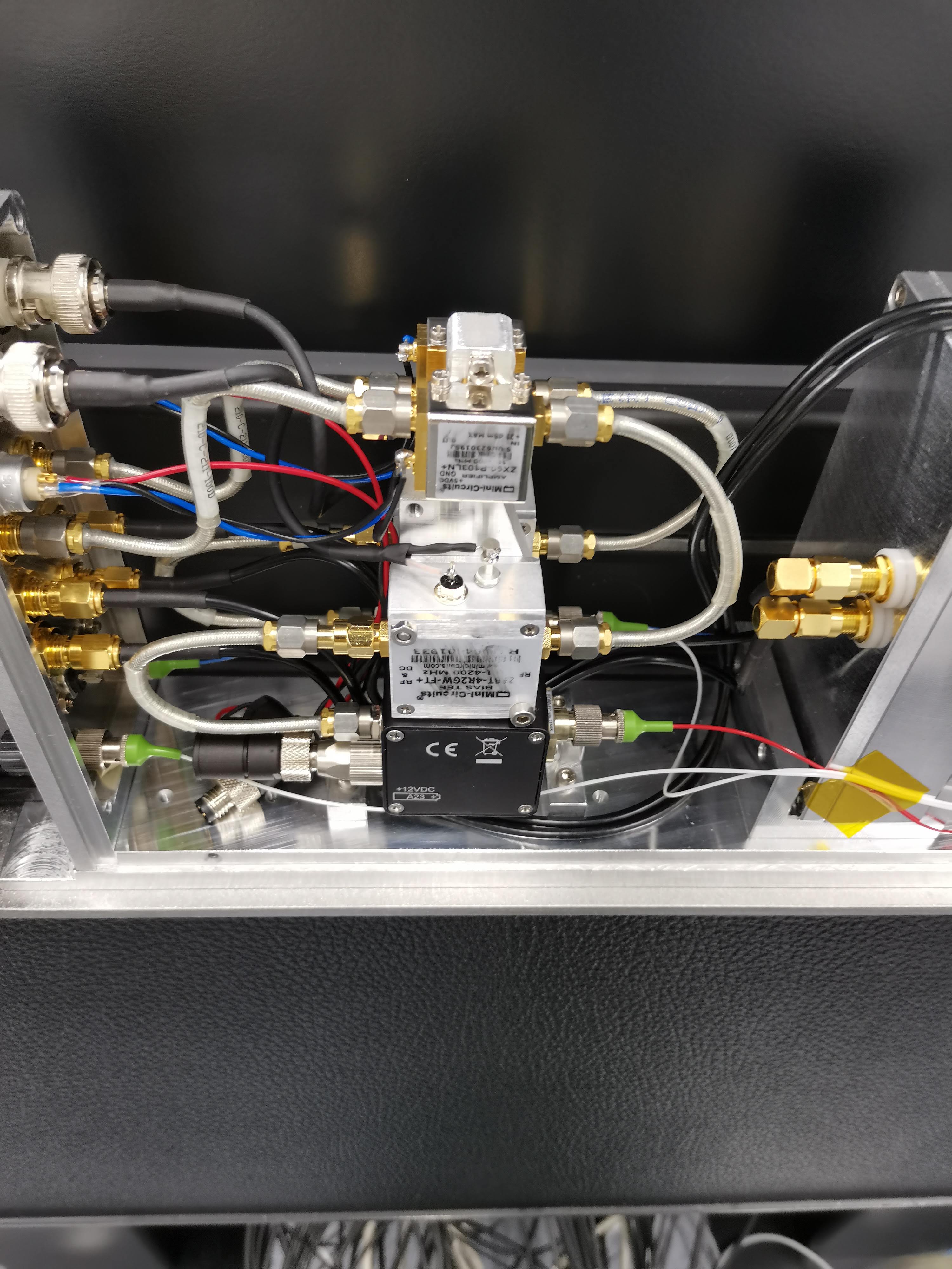
- SC PLL: the SQZ Main Laser and the SC Laser Pick off are superposed with a fibered beam splitter ( Thorlabs: PN1064R5A2 ). The two photodiode used for the beat note detection are commercial (Thorlabs DET08CFC/M). The output of the photodiode is blended (RF + DC), the two are divided exploiting a bias tee (Minicircuit ZFBT-4R2GW-FT+) and then RF signal is amplified with a Minicircuit ZX60-P103-LN+ amplifier (+13dB of amplification at about 1.2 GHz, i.e. SC PLL working frequency).
Modification of the Main PLL Amplifier respect to O3:
- Change of the sensor: from a free space sensor to a pig tailed sensor
- The Mixer for the on board demodulation is no more bypassed
- The buffer for the DC signal extraction is installed
Input output of the box
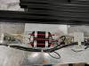
Main PLL side (figure 4): from the top:
- the diaphragm and the input for the SQZ Main Laser,
- 2 Output for the PD demodulated signal for online phase noise measurement,
- 2 Lemo 6 connectors used to power the two PD Amplifiers,
- 2 BNC connector for the PD DC signal extraction,
- a spare Fiber input connector
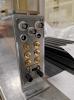
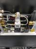
SC PLL side (figure 5): from the top
- 2 BNC for the DC signal extraction,
- a spare BNC,
- 2 Lemo 6 connector to power the two thorlabs photodiode and the Minicircuit Amplifier,
- 2 SMA connector for the RF signal extraction of the SC PLLs,
- 2 SMA connector for the RF Signal extraction for the Main PLL,
- 2 SMA connector for the LO signal input for the on board demodulation of the main PLL
- A RS232 connector that can be used for a possible thermal control of the box
- 2 Fiber input for the PSL pick off and for the Main Laser Pick off
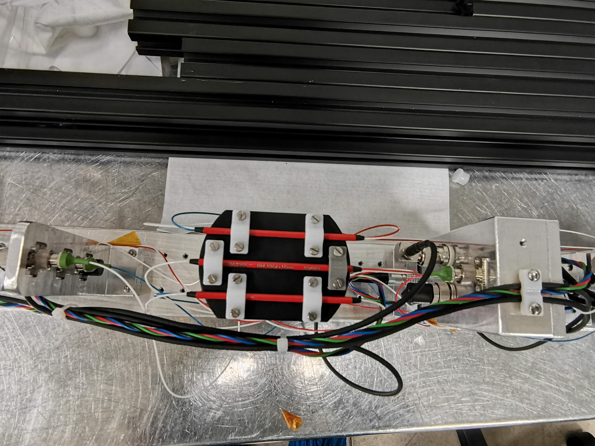
Fiber wrapping
The 11 optical fibers are wrapped on the plastic cylinder in the box. From the top we wrapped before the 3 fiber of the 50:50 splitter, then the 4 fiber of the SC PLL splitter and finally in the bottom part the 4 fibers for the Main PLL Beam splitter
In figure 6 the SQZ Main Laser splitter is in the center, the main PLL beam splitter is the one with the external white fiber, i.e. the first from the top in the foto (PSL Pick off Input) and the SC PLL beam splitter is the one with external blue fiber the last from the top in the photo (SC input)
The 11 optical fibers are blocked to the ciliner with a teflon tape.
Missing components:
The short RF cables used to connect the RF output of the SC PD to the amplifier, biase tee and the output panel
The box is ready to be installed on the bench and for the first tests
