We did some tests to investigate the flat noise problem.
The first point was to close the shutter of one of the two B1 photodiodes (B1 PD1 in particular) to check if the light scattered by the shutter had an effect on the flat noise level.
Keeping the SDB2_B1_PD1 shutter closed, we first changed the balance factor between the two photodiodes in the ITF_LOCK.ini file (b1_pd_balance) from 0.5154 to 0.0, which puts all the weight on B1_PD2, and in this configuration we acquired the lock in LN3.
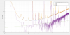
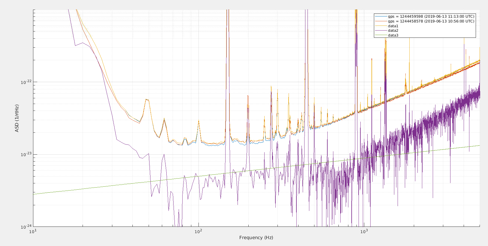
In this configuration we took data with two different DARM offset (DARM_SET = 6.5e-4 corresponding to ~2mW on B1_PD2 and DARM_SET = 8.8e-4 corresponding to ~2.75mW on B1_PD2 ), to see if there was any difference. The results are shown in the first plot, where the blue curve corresponds to 1.4mW on B1 PD2, the red curve to 2mW on B1 PD2 and the yellow to 2.8mW. The additional noise (violet curve) is added in quadrature when going from 1.4mW to 2.8mW, and matches the expectations that the flat noise increases by a factor sqrt(2), that is a noise of 5e-24*(f/100)^0.25 (green line). Notice that we disabled the squeezing not to risk to unlock because of the lack of B1_PD1.
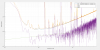
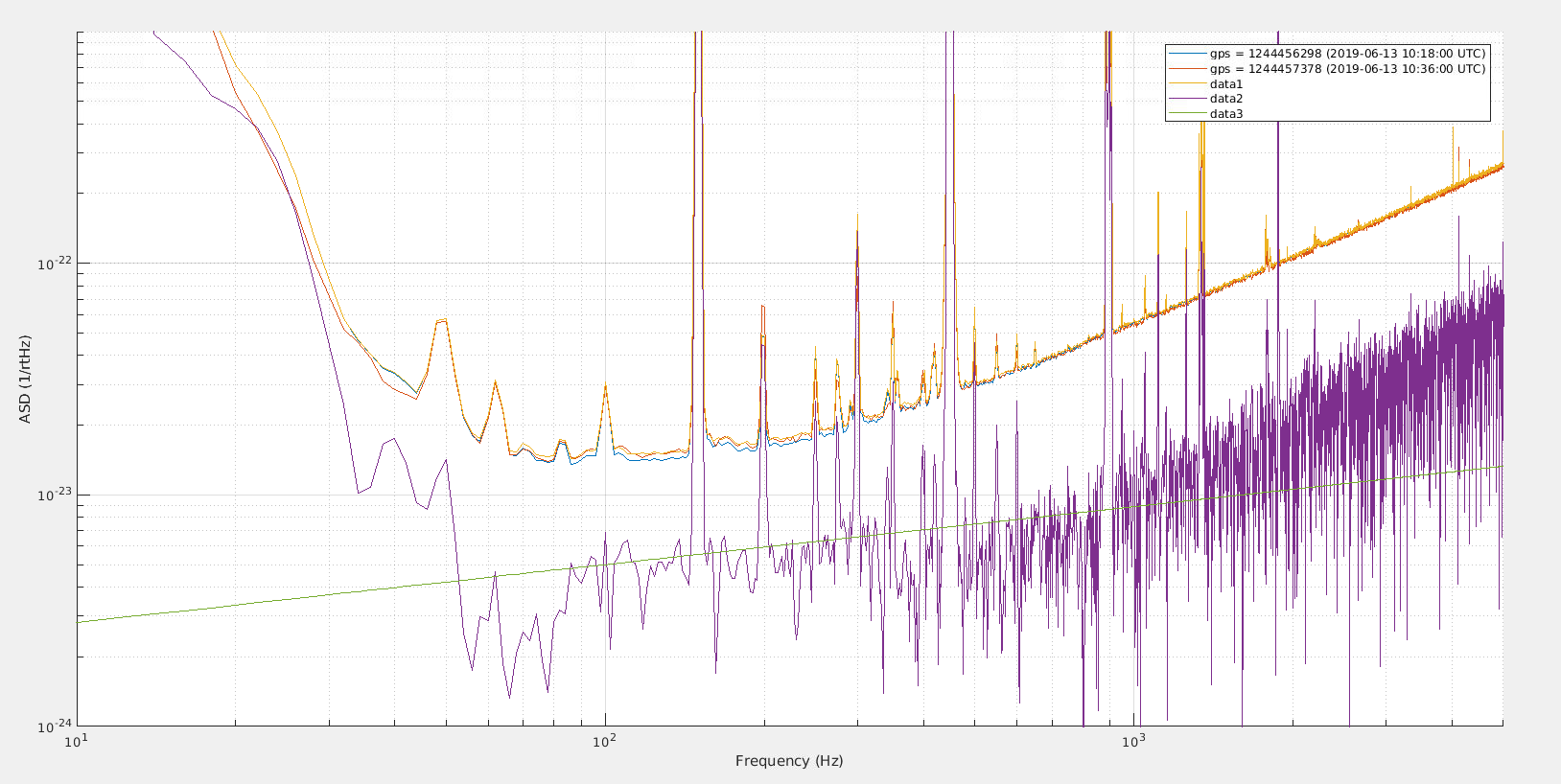
After that, we opened again the B1_PD1 shutter, without changing the balancing factor, and took a measurement also in this configuration in order to compare the conditions shutter open/closed. Also these measurements were performed without squeezing. Figure 2. For the same power level, the curves don't show significant differences.
Finally, we put back the original 2 PDs configuration and repeated the DARM offset scan: we did one point at DARM_SET = 8.8e-4, then decreased to DARM_SET = 4.5e-4 (which is the standard value), then decreased further to try and measure the contrast defect. In this configuration, we did DARM_SET =3e-4, DARM_SET =2e-4, DARM_SET =1e-4, but at this point the ITF unlocked and we couldn't take enough data before the end of the commissioning shift.
In the following the GPS start time, we stayed 15 minutes in each step:
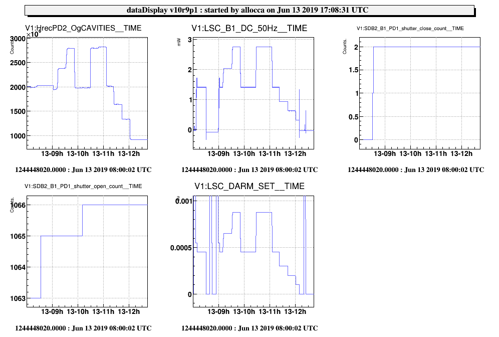
09:04 (4min) data with B1 PD1 shutter closed, 1.4mW on B1 PD2
09:12 (18min) 2mW on B1 PD2 (first 10min the Hrec OG and subtraction may not be up to date)
09:34 (16min) 2.75mW on B1 PD2 (first 10min the Hrec OG and subtraction may not be up to date)
09:52 (17min) 1.4mW on B1 PD2
10:11 (15min) 1.4mW on B1 PD2, B1 PD1 shutter open
10:29 (15min) 2.75mW on B1 PD2, B1 PD1 shutter open
10:48 (16min) 2.75mW on B1 PD2, 0.5 B1 PD balance, squeezing on
11:06 (16min) 1.4mW on B1 PD2, 0.5 B1 PD balance, squeezing on
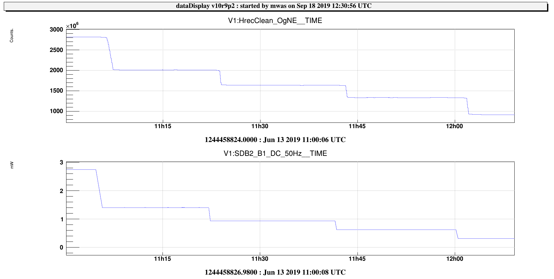
11:24 (17min) 0.98mW on B1 PD2, 0.5 B1 PD balance, squeezing on
11:42 (18min) 0.65mW on B1 PD2, 0.5 B1 PD balance, squeezing on
12:00(9 min) 0.31mW on B1 PD2, 0.5 B1 PD balance, squeezing on
UNLOCK
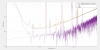
At a first glance, it seems that closing the B1 PD1 shutter doesn't have an effect on the flat noise, the flat noise is still present and seems to be at the expected level (5e-24*(f/100)^0.25 for the nominal dark fringe offset, and 7e-24*(f/100)^0.25 for the double power on the B1 PDs.
As a first conclusion, it seems that the flat noise still depends on the DARM offset and, therefore, on the dark port power.
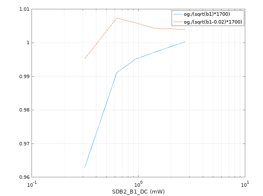
An estimation of the contrast defect will be performed later.
